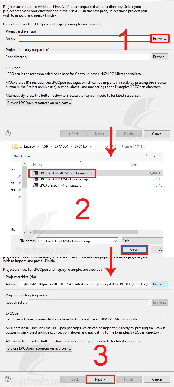
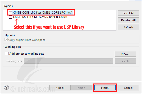
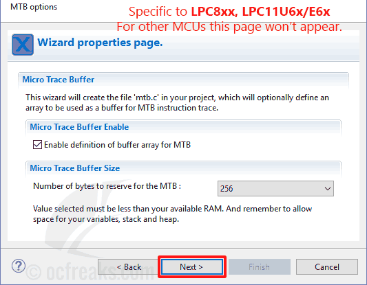
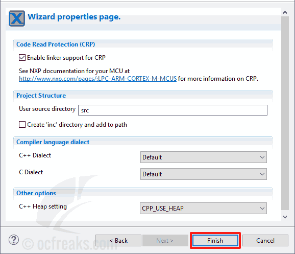
Quantcast
Channel: Embedded – OCFreaks!
Viewing all 57 articles
Browse latest View live

Hexadecimal and Binary Number System basics for Embedded Programming

$
0
0
To get started in Embedded programming following things need to be absolutely clear in our heads:
  1. Binary and Hexadecimal Number Systems.
  2. Interconversion of Binary and Hexadecimal.
  3. Bit Level Operations.
  4. Pointers , etc..

This tutorial mainly deals with Hexadecimal & Binary Numbering Systems and how to inter-convert them. This lays the foundation for bit level operations. A complete tutorial for bit level(or bitwise) operations is located @ www.ocfreaks.com/tutorial-embedded-programming-basics-in-c-bitwise-operations/.

Numbering Systems & Interconversion

Hexadecimal System / Base-16

The Hexadecimal number system is famous in computing world specially in digital electronics. Its base-16 because it uses 16 symbols to represent any number and each digit has an associated multiplication factor which is a power of 16. Its basically a ‘compact’ numbering system in which few digits are required to represent a sufficiently big number as compared to Decimal system. A Hexadecimal number can readily converted into a binary number and vice-verse. Digits in Hexadecimal systems are 0 to 9 and A,B,C,D,E,F. Each digit in a hexadecimal system can be represented using 4 binary digits. The order of the digits is in increasing power of 2. We will see Hexadecimal in detail but first lets go through Decimal and Binary numbering system & its conversion from binary to decimal.

Decimal System / Base-10

Decimal Numbering system or Base-10(technically) system : This the numbering system we use in our daily lives. Each digit in a decimal number has an associated ‘weight’ which is nothing but the base raised to the location number of the digit. Its Base-10 because it uses a combination of 10 ‘symbols’ or say digits(0,1,2,3,4,5,6,7,8,9) to represent any number.

Consider a decimal number 2734 : By default the digit on extreme RIGHT is called LSD or Least significant digit. In out case its ’4′. While the digit on extreme LEFT is called MSD or Most Significant Digit i.e ’2′ – It most significant because the change in digit at that location gives big changes in value of the number. Same argument is applicable for LSD. As you know that Units place has a multiplication factor of 1 , Tens has that of 10 , Hundreds has that of 100 and soo on.. similar to this we have multiplication factor for each digit in binary number system as well.

Binary System / Base-2

Binary Numbering system or Base-2 system: It used only 2 symbols(called bits) ’0′ & ’1′ to represent any number. On this Numbering or Counting System is computer understandable and hence most important for embedded programming though its very simple to understand. Binary system can be best understood by using an example to convert Binary to Decimal.

Lets take an example and try to understand binary to decimal conversion :

Consider a binary number say : 10011 which needs to be considered into decimal. Each bit in the binary number carries a specific multiplication factor or say ‘weight’ or say ‘order’. By default the bit on extreme right is starting or the 0th bit and that on the extreme left is last bit. Hence the 1st bit (technically – 0th since in computing counting starts from 0 and not 1 hence as called ’0 indexed’ system) from the right will have an order of 20 , next bit will have an order of 21 and so on.

Starting form the LSB i.e Least significant bit from RIGHT we multiply each bit with increasing power of 2 i.e. Bit 0(LSB) will be multiplied with 20 , Bit 1 multiplied with 21 , Bit 2 multiplied with 22 and on.

After this we simply add all products to get the converted number which is in Decimal.

In our case we have 5 digits hence our last power of 2 will be 24 with 20 begin the first :

Order / Multiplication Factor(MF) 24 23 22 21 20
Bit Value at each Position 0 1 0 1 1
Value times the Order/MF 24 x1 =16 23 x0 =0 22 x0 =0 21 x1 =2 20 x1 =1
Sum 16+0+0+2+1 =19

Now we simply add the above products to get Decimal of 01011.

Hence , Decimal_of(01011) = 16+0+0+2+1 = 19
Note : As with decimal , since 09 or 009 or 0009 mean ’9′(the leading zeros have no significance) , in binary system too 011 , 0011 , 00011 mean ’11′ since the leading zeros have no meaning and can be discarded.

Similar to above is conversion from Binary to Hexadecimal as follows:

Recall that each Hexadecimal Digit is represented by ‘exact’ 4 bits. Hence ’4′ is a very important number in this case. A group of 4 bits is called a Nibble and that of 8 bits is called a Byte. So in hexadecimal basically we deal with Nibbles.


First , Lets have a look at the conversion chart below for Decimal, Hexadecimal and Binary:

Decimal Hexadecimal Binary
0 0 0000
1 1 0001
2 2 0010
3 3 0011
4 4 0100
5 5 0101
6 6 0110
7 7 0111
8 8 1000
9 9 1001
10 A 1010
11 B 1011
12 C 1100
13 D 1101
14 E 1110
15 F 1111

From simple observation we can deduce the fact that : to convert any binary number to hexadecimal we need to first group the bits where each group contains 4 bits and then directly replace that group with its equivalent hexadecimal from the above table. We start the grouping from LSB i.e from right.

Also the binary representation of any hexadecimal ‘symbol’ or ‘digit’ has only 4 ‘orders’ or ‘weights’ or ‘multiplication factor’ associated. These are 23 , 22 , 21 and 20 or simply 8-4-2-1.

Consider a binary number : 1010101001110 , we can group it as 10-1010-0100-1110. Note that the grouping into 4 starts from right side. Now the group on the extreme left has only 2 bits so we can append zeros to keep things straight forward.

Hence we get : 0010-1010-0100-1110 , Now we replace each group by its Hex representation.

Binary => 0010 1010 0100 1110
Hexadecimal => 2 A 4 E

Hence Hexadecimal_of(1010101001110) = 2A4E

Converting Hexadecimal to Binary: This is as simple as counting 1,2,3 :P . Simply replace each Hexadecimal digit with its binary equivalent.. Thats it!

For eg. consider a Hex number say B39F1A

Replacing Each Hex digit with its binary equivalent we get :

Hexadecimal Digit B 3 9 F 1 A
Binary equi. of each Hex Digit 1011 0011 1001 1111 0001 1010

Hence Binary_of(B39F1A) = 101100111001111100011010
Note that each digit is replaced with exact 4 bits .. i.e 3 is replaced by 0011 and not ’11′. Replacing it with ’11′ will change the value of the number. Also this method is NOT applicable for conversion from Decimal to binary.

Tutorial : Embedded programming basics in C – bitwise operations

$
0
0
Bitwise or bitlevel operations form the basis of embedded programming. A knowledge of Hexadecimal and Binary Numbering system is required along with conversion from binary to hex and vice-verse. A tutorial for that is located @ www.ocfreaks.com/hexadecimal-and-binary-number-system-basics-for-embedded-programming/. If you are less familiar with hexadecimal and binary number systems that will help you.

Further , I assume that the reader has a basic understanding of C programming language , Digital Logic , MCU(Registers,etc..).

Embedded Programming Basics : Bit level Operations in C:

Now getting armed with the knowledge of interconversion between Hexadecimal and Binary we can start with Bitwise(or bit level) operations in C. There are bascially 6 types of Bitwise operators. These are :
1. Bitwise OR operator denoted by ‘|
2. Bitwise AND operator denoted by ‘&
3. Bitwise Complement or Negation Operator denoted by ‘~
4. Bitwise Right Shift & Left Shift denoted by ‘>>‘ and ‘<<‘ respectively
5. Bitwise XOR operator denoted by ‘^

Important Note: Bitwise Operations are meant to be done on Integers only! No Float and No Double here plz!

Below is the Truth table for OR , AND , XOR – each of them require 2 operands:

Operand 1(OP1) Operand 2(OP2) OP1 | OP2 (OR) OP1 & OP2 (AND) OP1 ^ OP2 (XOR)
0 0 0 0 0
1 0 1 0 1
0 1 1 0 1
1 1 1 1 0

Hexadecimal Numbers in C/C++ program have a ’0x’ prefix and for Binary we have a ’0b’ prefix. Without these prefix any number will be considered as a Decimal number by the compiler and hence we need to be explicit with numbers.
Note : Implied Declaration and Use of Numbers when working at bit level -

Consider: int n = 0x7F2; Here its is implied that n will be 0x000007F2 since n is a 32bit number. Here number will be automatically padded with Zeros form right hand side as required.

Consider : int x = 0b1010; Here too zeros (28 0s) will be padded on the left to make x 32bit.

Consider: int n = (1<<3); Here the 3rd bit will be 1 and rest all will be made zeros by the compiler.

In short 0s are padded towards the left as required.

Consider there is a 32 bit register which is connected to 32 pins. Changing any bit to 1 will produce a HIGH (LOGIC 1) and making it ’0′ will produce a LOW i.e LOGIC 0 on the corresponding bit. If we assign bit number 19(from right) a ’1′ then pin 19 will produce a HIGH.

In C this can be done as :

REG = 0b0000000000010000000000000000000; //binary
REG = 0b10000000000000000000; //same as above since leading 0s will be automatically padded

=or=

REG = 0x00100000; //hexadecimal

=or=

REG = (1<<19); // sort of compact binary rep.


As you can see using binary number directly is a headache – specially when there are like 32 bits to handle. Using Hexadecimal instead makes it a bit easier and using Left shift operator makes it super simple. Here ‘<<' is called the Left Shift Operator. Similar to this is ">>” viz. Right Shift operator.

(1<<19)” Simply means ‘Shift 1 towards the LEFT by 19 Places‘. Other bits will be Zero by default.

We generally use Hexadecimal when we need to change bits in bluk and Left shift operator when only few bits need to be changed or extracted.

ORing in C:

This is the same exact thing as in Digital Logic i.e 1 ORed with ‘x’ is always 1 and 0 ORed with ‘x’ is always ‘x’ , where x is a bit. Lets take two 4-bit numbers and OR them. Consider two 4-bit numbers n1=0100 & n2=1001. Here the 1st bit of n1 will be ORed with 1st bit of n2 , 2nd bit of n1 will be ORed with 2nd bit of n2 and soo on. In this case n1 is decimal 4 and n2 is decimal 9.

n1 (4) => 0 1 0 0
n2 (9) => 1 0 0 1
ORed Result (13) => 1 1 0 1

Hence we get 4 | 9 = 13.
It can be seen that bitwise ORing is similar to addition but this is not always the case since bitwise OR doesnt deal with carry generated after adding(i.e ORing) two 1s. For e.g. 12 | 9 is also = 13.

Now , If we want to make bit 19 and 12 as ’1′ we can use the binary OR operator which is represented by a pipe i.e ‘|’.

REG = (1<<19) | (1<<12); // 19th and 12th bits are set to '1' , rest are Zeros.

Now consider we want to making the first 21 bits (from right) to ’1′. This is can be done using hexadecimal notation instead of using shift operator since we will need to write 21 left shift operations for each of the 21 bits. In this case just consider we have a 32 bit number which has all first 19 bits ’1′. Then convert this number to hexadecimal and use it!

REG = 0x003FFFFF;

Hence using Hexadecimal or Binary operator depends on the situation.

Bitwise 1′s Complement / Negation in C :

Now lets say.. we need to convert all 0s to 1s and vice-verse. This can be done using the Bitwise negation operator denoted by ‘~’. The result of this operation is called 1′s Complement. Its also called a ‘NOT’ operation. ‘~’ is a unary operator since it requires only 1 operator while rest all are binary operators.

1st lets take a 4bit example to keep it simple.
Consider a binary number 1101. Its Negation will be ~(1101) => 0010.

Now lets get back to 32 bit numbers.. In C it can be done as follows:

int x = 0x0FFF000F;
REG = ~(x); // REG is assigned 0xF000FFF0;

=or=

REG = ~(0x0FFF000F); // REG is assigned 0xF000FFF0;

ANDing in C:

Binary AND operator in C is denoted by ‘&’. When 2 numbers are ANDed each pair of ‘corresponding’ bits in both numbers are ANDed. Consider two 4-bit binary numbers ANDed : 1010 & 1101 , here nth bit of both numbers are ANDed to get the result. Here the same truth table(already shown above) is followed as in Therotical Digital Logic i.e 1 ANDed with x is always ‘x’ (x is a binary number.. a bit) and 0 ANDed with ‘x’ is always 0.

char n1,n2,n3; //we can declare an 8-bit number as a char;
n1 = 0xF4; // binary n1 = 0b11110100;
n2 = 0x3A; // binary n2 = 0b00111010;
n3 = n1 & n2; // binary n3 = 0b00110000; i.e 0x30;

XORing in C:

XOR is short for eXclusive-OR. By definition of XOR , the result will be a ’1′ if both the input bits are different and result will be ’0′ if both are same (as seen in the table few paragraphs above). XOR can be used to check the bit difference between 2 numbers or Registers.

int n1,n2,n3;
n1 = 0b10011;
n2 = 0b11010;
n3 = n1^n2; // n2 = 0b01001;

Working with Read/Write Registers in C:

Generally its a bad Idea to assign a value directly to Registers since doing so may change the value of other bits which might be used to contol some other hardware.

Consider an 8 bit Register say REGT_8b is used to Start/Stop 8 different Timers. Bit 0 (from left) controls Timer 0 , Bit 1 Controls Timer 1 and so on… Writing a ’1′ to a bit will Start the timer and a ’0′ will Stop the Timer.

Now lets say Timers 7,6,5 are started and others are stopped. So the current value of REGT_8b will be ‘11100000‘. Now assume that we want to Start Timer 2. We can do this in a manner which doesnt affect the other bits as follows :

REGT_8b = REGT_8b | (1<<2); // which is 11100000 | 00000100 = 11100100

=or simply=

REGT_8b |= (1<<2); // same as above


Now lets say we want to Stop Timer 6. This can be achieved as follows :
REGT_8b = REGT_8b & (~(1<<6));

=or simply=

REGT_8b &= ~(1<<6);


Here (1<<6) will be 01000000 (considering it 8bit.. for 32 bit 0s will be padding on left). Then ~(1<<6) will be ~(01000000) = 10111111 and finally when its ANDed with current value of REGT_8b 6th bit of REGT_8b will be set to ’0′ and others will remain as they were since ANDing any bit with 1 doesn’t change its value.

More Examples :

For below examples assume current value of REGT_8b as ’11100011′ which is 8 bit.

1) Stop Timers 0 and 5 :

REGT_8b &= ~( (1<<0) | (1<<5) );

=> ((1<<0) | (1<<5)) is = ((00000001) | (00100000)) = 00100001
=> ~(00100001) is = 11011110
=> Finally REGT_8b & 11011110 is = (11100011) & (11011110) = 11000010 => Timers 0 and 5 Stopped!


2) Start Timers 3 and 4:

REGT_8b |= ( (1<<3) | (1<<4) );

=> ((1<<3) | (1<<4)) is = ((00001000) | (00010000)) = 00011000;
=> Now REGT_8b | (00001000) is = (11100011) | (00011000) = 11111011 => Timers 3 and 4 Started!


3) Stop Timer 7 and Start timer 3:

REGT_8b = (REGT_8b | (1<<3)) & (~(1<<7));

Above complex expression can be avioded by doing it in 2 steps as:

REGT_8b &= ~(1<<7); // Stop Timer 7
REGT_8b |= (1<<3); // Start Timer 3

Monitoring Specific bit change in Registers :

Many times we need to read certain Flags in a register that denotes change in Hardware state. Consider a 32 bit Register REGX in which the 12th bit denotes the arrival of data from UART Receive pin into buffer. This data may be a command for the MCU to start or stop or do something. So we need to read the command then interpret it and call appropriate function. In simplest approach we can continuously scan for change in 12th bit of REGX as follows :

while( REGX & (1<<12) ) // monitor for 12th bit changing from 0 to 1
{
...
...
}

Unless the 12th bit of REGX is ’1′ the result of (REGX & (1<<12)) will always be zero. When 12th bit is 1 then (REGX & (1<<12)) will be = (1<<12) which is obviously greater than 0 and hence is evaluated as TRUE condition and the code inside the while loop gets executed.

To monitor for the change in 12th bit from 1 to 0 we just Negate the condition inside while to :

while ( ~(REGX & (1<<12)) )// monitor for 12th bit changing from 1 to 0
{
...
...
}

Extracting/Testing Bit(s) from a Register:

To extract a bit from a register we can use a variable in which all other bit locations , except the one we are intereseted in , are forced to 0. This can be done using masks.

Lets assume we want to extract bit number 13. For this we first define a mask in which bit location 13 is 1 and rest are all zeros. Then we AND this mask with the register and save the result in a variable.

int mask ,extract_n;
mask = (1<<13);
extract_n = REGX & mask; // bit 13 goes to extract_n


If the 13th bit of REGX was 1 then the 13th bit of extract_n will also be one. Similarly for 0. This can be easily extended to extract multiple bits.

To test whether bit 13 of REGX is 0 or 1 we can accomplish it as follows :

if(REGX & (1<<13))
{
...
...
}


This is similar to what we did using mask and monitoring except that the result here is used as condition for ‘if’ construct. Here too ‘(REGX & (1<<13))‘ will evaluate to true if bit 13 is 1 and false if bit 13 is 0.

LPC2148 GPIO Programming Tutorial

$
0
0

When getting started in embedded programming, GPIO (viz. General Purpose Input Output) pins are one of the first things played with. Its also quite evident that the most popular “hello world” program in embedded systems programming is Blinky i.e a LED connected to pin on the Microcontroller that keeps blinking. The use of GPIO is not limited to driving LEDS but can be also use for reading digital signal , generating triggers for external components , controlling external devices and what not. In this tutorial we see how to use and program GPIO Pins for lpc214x ARM 7 microcontrollers from NXP/Philips.

Before getting into this you need to have basic understanding of Binary and Hexadecimal system and Bitwise operations in C.
*=>Guide to Binary and Hexadecimal system is @ Hexadecimal and Binary Number System basics for Embedded Programming.
*=>Tutorial for Bitwise Operations in C is @ Tutorial : Embedded programming basics in C – bitwise operations.

I’ll use lpc2148 MCU (having 32-bit ARM 7 CPU) for explanation and programming examples. The Programs and Register names that I have shown are used in KEIL. You can download KEIL UV4 from here. If you are using a different IDE/Compiler then you’ll need to change the Register Names as required. Also do note that Integer Data-Type i.e. an ‘int’ is always 32 bits in KEIL when programming for 32bit ARM7 MCUs like lpc2148.

Most of the function oriented pins on lpc214x Microcontrollers are grouped into ports. lpc2148 has 2 ports viz. Port 0 and Port 1.

  • Port 0 is a 32 bit wide I/O port (i.e it can be used for max 32 pins where each pin refers to a corresponding bit) and has dedicated direction bits for each of the pins present in the port. 28 out of the 32 pins can be used as bi-directional I/O (digital) pins. Pins P0.24 , P0.26 & P0.27 are unavailable for use and Pin P0.30 can be used as output pin only.
  • Port 1 is also a 32 bit wide I/0 port but Pins 0 to 15 i.e P1.0 – P1.15 are unavailable for use and this port too has a dedicated direction bit for each of the usable pins.
Note #1: The naming convention for Pins on MCU is ‘Px.yz’ where ‘x’ is the port number , 0 or 1 in our case since we have only 2 ports to play with in lpc214x , and ‘yz’ is simply the pin number in port ‘x’. For example : P0.2 refers to Pin number 2 of Port 0 , P1.13 refers to Pin number 13 in Port 1.

In lpc214x MCUs most of the PINS are Multiplexed i.e. these pins can be configured to provide different functions. I’ll explain this in upcoming tutorial. For now Just keep in mind that by default : all functional pins i.e pins in port 0 & 1 are set as GPIO so we can direclty use them when learning GPIO usage.

Note #2: The functions of the Pins in Port 0 & 1 can be selected by manipulating appropriate bits in PINSEL0/1/2 registers. Explaining this is outside the scope of this article and will be dealt in detail in another article. Just remember that assigning ’0′ to these registers forces the corresponding pins to be used as GPIO. Since by default all pins are configured as GPIOs we dont need to explicitly assign zero value to PINSELx registers in our programming examples.

Now , lets go through the registers used for GPIO programming.

1. IOxPIN (x=port number) : This register can be used to Read or Write values directly to the pins. Regardless of the direction set for the particular pins it gives the current start of the GPIO pin when read.

2. IOxDIR : This is the GPIO direction control register. Setting a bit to 0 in this register will configure the corresponding pin to be used as an Input while setting it to 1 will configure it as Output.

3. IOxSET : This register can be used to drive an ‘output’ configured pin to Logic 1 i.e HIGH. Writing Zero does NOT have any effect and hence it cannot be used to drive a pin to Logic 0 i.e LOW. For driving pins LOW IOxCLR is used which is explained below.

4. IOxCLR : This register can be used to drive an ‘output’ configured pin to Logic 0 i.e LOW. Writing Zero does NOT have any effect and hence it cannot be used to drive a pin to Logic 1.

Note #3: Naming convention for GPIO related registers – Replace ‘x’ with the port number to get the register name. For e.g IOxPIN becomes IO0PIN when used for Port 0 and IO1PIN when used to port 1. These are defined in ‘lpc214x.h’ header file for KIEL IDE.

Registers Names defined in ‘lpc214x.h’ header file are basically pointers which point to actual register in Hardware. Since lpc214x MCUs are 32 bit , the size of the pointer is also 32 bits. Each bit in these registers mentioned above is directly linked to a corresponding Pin. Manipulating these bits changes the behavior or state of the pins. For e.g consider IOxDIR register. Bit 0 of IO0DIR corresponds to pin 0 or port 0 hence bit ‘y’ in IOxDIR corresponds to pin ‘y’ in port ‘x’.

Now setting PIN 2 of Port 0 i.e P0.2 as output can be done in various ways as show :

CASE 1. IO0DIR = (1<<2); //(binary – direct assign: other pins set to 0)

CASE 2. IO0DIR |= 0×0000004; // or 0×4; (hexadecimal – OR and assign: other pins not affected)

CASE 3. IO0DIR |= (1<<2); //(binary – OR and assign: other pins not affected)

First thing is to note that preceding Zeros in Hexadecimal Notation can be ignored since bcoz have no meaning since we are working with unsigned values here (positive only) which are assigned to Registers. For eg. ’0×32′ and ’0×032′ and ’0×0032′ all mean the same.

Note #4: Note that bit 31 is MSB on extreme left and bit 0 is LSB on extreme right i.e Big Endian Format. Hence bit 0 is the 1st bit from right , bit 1 is the 2nd bit from right and so on.

Also note that the BIT and PIN Numbers are Zero(0) indexed which is quite evident since Bit ‘x’ refers to (x-1)th location in the corresponding register.

Case 1 must be avoided since we are directly assigning a value to the register. So while we are making P0.2 ’1′ others are forced to be assigned a ’0′ which can be avoided by ORing and then assigning Value.
Case 2 can be used when bits need to be changed in bulk and
Case 3 when some or single bit needs to be changed.

Also Note: All GPIO pins are configured as Input after Reset by default!

Example #1)

Consider that we want to configure Pin 19 of Port 0 i.e P0.19 as Ouput and want to drive it High(Logic 1). This can be done as :

IO0DIR |= (1<<19); // Config P0.19 as Ouput
IO0SET |= (1<<19); // Make ouput High for P0.19

Example #2)

Making output configured Pin 15 High of Port 0 i.e P0.15 and then Low can be does as follows:

IO0DIR |= (1<<15); // P0.15 is Output pin
IO0SET |= (1<<15); // Output for P0.15 becomes High
IO0CLR |= (1<<15); // Output for P0.15 becomes Low

Example #3)

Configuring P0.13 and P0.19 as Ouput and Setting them High:

IO0DIR |= (1<<13) | (1<<19); // Config P0.13 and P0.19 as Ouput
IO0SET |= (1<<13) | (1<<19); // Make ouput High for P0.13 and P0.19

Example #4)

Configuring 1st 16 Pins of Port 0 (P0.0 to P0.15) as Ouput and Setting them High:

IO0DIR |= 0x0000FFFF; // Config P0.0 to P0.15 as Ouput
IO0SET |= 0x0000FFFF; // Make ouput High for P0.0 to P0.15

Now lets play with some real world examples.

Example #5)

Blinky Example – Now we repeatedly make all pins in port 0 (P0.0 to P0.30) High then Low then High and so on. You can connect Led to some or all Pins on Port 0 to see it in action. Here we will introduce some delay between making all pins High and Low so it can be noticed.

#include <lpc214x.h>

void delay(void);

int main(void)
{
    IO0DIR = 0xFFFFFFFF; // Configure all pins on Port 0 as Output
   
    while(1)
    {
        IO0SET = 0xFFFFFFFF; // Turn on LEDs
        delay();
        IO0CLR = 0xFFFFFFFF; // Turn them off
        delay();
    }
    return 0; // normally this wont execute
}  

void delay(void)
{
    int z,c;
    c=0;
    for(z=0; z<4000000; z++) // You can edit this as per your needs
    {
        c++; // something needs to be here else KEIL compiler will remove the for loop!
    }
}

Example #6)

Configuring P0.7 as Input and monitoring it for a external event like connecting it to LOW or GND. P0.30 is configured as output and connected to LED. If Input for P0.7 is a ‘Low’ (GND) then output for P0.30 is made High which will activate the LED and make it glow (Since the other END of LED is connected to LOW i.e GND). Since internal Pull-ups are enabled the ‘default’ state of the pins configured as Input will be always ‘High’ unless it is explicitly made ‘Low’ by connecting it to Ground. Consider one end of a tactile switch connected to P0.7 and other to ground. When the switch is pressed a ‘LOW’ will be applied to P0.7. The setup is shown in the figure below:

#include <lpc214x.h>

int main(void)
{
    IO0DIR &= ~((1<<7)) ; // explicitly making P0.7 as Input - even though by default its already Input
    IO0DIR |= (1<<30); // Configuring P0.30 as Output

    while(1)
    {
        if( !(IO0PIN & (1<<7)) ) // Evaluates to True for a 'LOW' on P0.7
        {
            IO0SET |= (1<<30); // drive P0.30 High
        }
    }
    return 0; // this wont execute ever :P
}

Explanation:

‘(1<<7)' is simply 7th bit '1'(i.e 0x00000080) & rest all bit are zeros. When ‘(1<<7)' is ANDed with IO0SET it will make all other bits except 7th bit to '0'. The Value of 7th bit in result will now depend on IO0PIN's 7th bit. If its 1 (which means input is High) then result after ANDing will be 0×00000080 which is greater than zero and hence will evaluate to ‘TRUE‘. Also when we use ‘Logical NOT‘ i.e ‘!‘ then ‘!(TRUE)‘ evaluates to FALSE hence code is not executed for High Input. When P0.7 is given ‘Low’ the corresponding bit in IO0PIN i.e 7th bit will be set to 0. In this case the result of ‘IO0PIN & (1<<7)‘ will be ’0×0′ which evaluates to FALSE. Hence ‘!(FALSE)‘ evalutes to TRUE and code inside ‘if’ block gets executed.

BTW:The above while loop can be re-written as :

while( IO0PIN & (1<<7) )
{
    IO0SET |= (1<<30); // drive P0.30 High
}

For now lets stick to the original while loop since it keeps things simple.

Note #5: Since LPC214x runs on 3.3 Volts a High on any pin is (and must be) always 3.3 Volts while Low or GND is 0 Volts. Applying an input of more than 3.3 Volts like 5 Volts will permanently damage the pin! I have a couple of pins damaged on a few lpc214x boards due to this – that was when I was learning embedded stuff.
Example #7)

Now we will extended example 6 so that when the button is pressed the LED will glow and when released or not pressed the LED wont glow. Capturing inputs in this manner, using switches, leads to a phenomenon called ‘bouncing‘ which needs to be resolved using ‘debouncing‘ as explained below. We will a ‘flag’ variable to swtich between High and Low states.

Bouncing:

Usually in switches there are Metal contacts which Open and Close. Consider an Open switch. When it is closed the signal passes over initially and then briefly the contacts might loosen and possibly result in a Open-Circuit momentarily hence signal doesnt pass over for that short period of time. After this the contacts settle and signal passes over again ‘steadily’. This tendency of the metal contacts is referred to as ‘Bouncing’.

Debouncing:

Bouncing needs to be given special attention while processing/capturing inputs. Bouncing can be eliminated using ‘Debouncing’. Debouncing can be tackled at hardware or software level. In hardware it can be done using RC circuits , Latches , etc.. For the sake of this article I’ll show how to deal with it using software. In this we will sample(read) P0.7 status/state two times with a very brief delay in between. In our case this simple strategy is sufficient to prevent bouncing. Note that delay must be correctly chosen – it must not be too high nor too low. If the state of pin is same after taking the second sample then we can say that the new state of the pin is indeed stable.

I would recommend visiting the following links for understanding debouncing indepth.
1) www.ganssle.com/debouncing.htm
2) www.labbookpages.co.uk/electronics/debounce.html
3) www.eng.uwaterloo.ca/~tnaqvi/downloads/DOC/sd192/SwitchDebouncing.htm

#include <lpc214x.h>

void tiny_delay(void);

int main(void)
{
    int flag=0, pinSamplePrevious, pinSampleCurrent;
    IO0DIR &= ~((1<<7));
    IO0DIR |= (1<<30);
   
    pinSamplePrevious = IO0PIN & (1<<7); //Initial Sample

    while(1)
    {
        pinSampleCurrent = IO0PIN & (1<<7); //New Sample
       
        if( pinSampleCurrent != pinSamplePrevious )
        {
            //P0.7 might get low or high momentarily due to noise depending the external conditions or some other reason
            //hence we again take a sample to insure its not due to noise
           
            tiny_delay(); // momentary delay
           
            // now we again read current status of P0.7 from IO0PIN
            pinSampleCurrent = IO0PIN & (1<<7);
           
            if( pinSampleCurrent != pinSamplePrevious )
            {
                //State of P0.7 has indeed changed
                if(flag) //First time Flag will be = 0 hence else part will execute
                {
                    IO0SET |= (1<<30); // drive P0.30 High
                    flag=0; //next time 'else' part will excute
                }
                else
                {
                    IO0CLR |= (1<<30); // drive P0.30 Low
                    flag=1; //next time 'if' part will excute
                }
               
                //set current value as previous since it has been processed
                pinSamplePrevious = pinSampleCurrent;
            }
        }
    }
    return 0; // this wont execute ever :P
}

void tiny_delay(void)
{
    int z,c;
    c=0;
    for(z=0; z<1500; z++) //Higher value for higher clock speed
    {
        c++;
    }
}

Explanation:

Initially P0.7 will be high since pull-ups are enabled. Hence ‘pinSamplePrevious‘ and ‘pinSampleCurrent‘ will have same value and ‘if‘ will evalute to false so code inside wont execute.

Event #1) Pressing switch: When switch is pressed P0.7 will now be ‘Low’ but this might be due to noise or glicthy contact in switch so we again read the value of P0.7 to confirm that the new state of P0.7 is stable. If it is stable then value of ‘pinSampleCurrent’ will differ from ‘pinSamplePrevious’ and the inner ‘if‘ block evalute to true and code inside will execute. When its executed first time ‘flag‘ will be 0. Hence, ‘if(flag)‘ will be false and ‘else‘ block will execute which will drive P0.30 Low and set flag to ’1′.

Event #2) Releasing switch: Now After the switch has been released the value of P0.7 will change to ’1′ i.e High. Previous state was ‘Low’ and current is ‘High’ hence pinSamplePrevious’ and ‘pinSampleCurrent’ will again differ and in similar manner as above the code inside inner ‘if’ block will execute. This time though , since flag is 1, ‘if(flag)‘ will evaluate to true and P0.30 will be set to High i.e ’1′ and flag will be set to 0.

Improvising play with Bits:

Using the left shift operation is not confusing but when too many are used together I find it a little bit out of order and affects code readability to some extent. For this I define a Macro ‘BIT(x)’ which replaces ‘(1<<x)’ as:

#define BIT(x) (1<<x)

After that is defined we can directly use BIT(x). Using this Example 3 can be re-written as:

IO0DIR |= BIT(13) | BIT(19); // Config P0.13 and P0.19 as Ouput
IO0SET |= BIT(13) | BIT(19); // Make ouput High for P0.13 and P0.19


Example 6 can be re-written as:
#include <lpc214x.h>

#define BIT(x) (1<<x)

int main(void)
{
    IO0DIR &= ~(BIT(7));
    IO0DIR |= BIT(31);

    while(1)
    {
        if( !(IO0PIN & BIT(7)) )
        {
            IO0SET |= BIT(31);
        }
    }
    return 0;
}


TODO: Add some diagrams so its easy to understand what I’ve tried to explain.

If any reader wants to contibute to this article PM me on forums @ www.ocfreaks.com/forums/ Link to my profile on forums is here. Reader will get full credit he/she deserves for contribution :)

LPC214x PLL Tutorial for Cpu and Peripheral Clock

$
0
0

Introduction

PLL stands for Phase Locked Loop and is used to generate clock pulse given a reference clock input which is generally from a crystal oscillator(or XTAL). Configuring and using PLL in lpc124x MCUs is pretty simple and straight forward.

Lpc214x MCUs have 2 PLL blocks viz. PPL0 and PLL1. PLL0 is used to generate the System Clock which goes to CPU and on-chip peripherals while PPL1 is strictly for USB. PLL interrupts are only available for PLL0 and not for PLL1. Input clock to both the PLLs must be between 10Mhz to 25Mhz strictly. This input clock is multiplied with a suitable multiplier and scaled accordingly. But here we have a upper limit of 60Mhz which is the maximum frequency of operation for lpc214x MCUs. PLLs also contain CCOs i.e current controlled oscillators which we are not much concerned about … atleast in the case of lpc214x MCUs. CCOs operate in range of 156Mhz to 320Mhz and there is also a divider to force CCOs to remain in their range.

Basics

Lets define some symbols which are used in Datasheet and also which I’ll be using in this tutorial :

FOSC => frequency from the crystal oscillator(XTAL)/external clock
FCCO => frequency of the PLL Current Controlled Oscillator(CCO)
CCLK => PLL output frequency (CPU Clock)
M => PLL Multiplier value from the MSEL bits in the PLLCFG register
P => PLL Divider value from the PSEL bits in the PLLCFG register
PCLK => Peripheral Clock which is derived from CCLK

[Table 1]

Now , PLL output clock is given by the formula:
  • CCLK = M x FOSC
    =or=
  • CCLK = FCCO / (2 x P)

CCO output clock is given by:

  • FCCO = CCLK x 2 x P
    =or=
  • FCCO = FOSC x M x 2 x P


Note from Datasheet:

The PLL inputs and settings must meet the following:
  • FOSC is in the range of 10 MHz to 25 MHz.
  • CCLK is in the range of 10 MHz to Fmax (the maximum allowed frequency for the microcontroller – determined by the system microcontroller is embedded in).
  • FCCO is in the range of 156 MHz to 320 MHz.

Setting-up and using PLL

Here we’ll be focusing on PLL0. We’ll see PLL1 some other day since its not required at this moment. Explaining the internal working of PLLs and CCOs in detail is not in the scope of this tutorial. Here we are just concerned about its usage rather than knowing its internals. To play with PLLs we are given a Multiplier and a Divider which decide the output frequency/clock form PLL block. But we must play cautiously with PLLs since the CPU and other MCU peripherals operate on the clock provided buy it. So if PLL is deliberately or accidentally miss-configured the MCU may go nuts! Miss configuring it deliberately is the sole responsibility of the user and not us ;P Now .. to handle the accident part .. we have a got a FEED Sequence which needs to be issued whenever we wanna configure PPL. You can visualize this by imagining PLL to be enclosed in a safe or a locker. To access PLL we need to have a key to open the safe in order to use or configure it. The key here is the ‘Feed Sequence’. Feed Sequence is nothing but assignment of 2 particular ‘fixed’ values to a register related to the PLL block. This register is called ‘PLL0FEED’. And those fixed values are 0xAA and 0×55 are ‘in order’!. Hence the code for feed sequence must be :

PLL0FEED = 0xAA;
PLL0FEED = 0x55;

Now , lets see the other PLL Registers we can use:

1)PLLxCON:(x= PLL block 0 or 1) This is the PLL Control register used to enable and ‘connect’ the PLL. The first bit is used to ‘Enable’ PLL. The second bit is used to ‘Connect’ the PLL.
Note #1: Initially when the MCU boots-up it uses its internal RC Oscillator as clock source. When the PLL is setup and enabled we must switch from internal RC Oscillator to the PLL’s output clock. This is referred to as ‘Connecting’ the PLL. PLL is only connected when both ‘Enable’ and ‘Connect’ bits are 1 and a valid feed sequence is applied.

2)PLLxCGF: The multiplier and divider values are stored in this register. The 1st 5 bits (called MSEL) are used to store the Multiplier(M). Next 2 bits i.e 5,6 (called PSEL) are used to store the value of the Divider(P).

3)PLLxSTAT: This is a read only register and contains current status of PLL enable , connect , M and P values. You can read more about the bits in datasheet – page #37. We are more interested in the 10th bit of PLLxSTAT since it contains the lock status. When we setup and enable the PLL it takes a while for PLL to latch on the target frequency. After PLL has latched or locked to target frequency this bit becomes 1. Only after this we can connect PLL to the CPU. Hence , we need to wait for PLL to lock on to target frequency.

The Order of setting up PLLs is strictly as follows :
  1. Setup PLL
  2. Apply Feed Sequence
  3. Wait for PLL to lock and then Connect PLL
  4. Apply Feed Sequence

Note that we have to apply Feed Sequence strictly as mentioned above.

Calculating PLL Settings

#1) PLL0

  1. Select the CPU Frequency. This selection may be based many factors and end application. On Chip peripheral devices may be running on a lower clock than the processor.
  2. Choose an oscillator frequency (FOSC). CCLK must be the whole (non-fractional) multiple of FOSC. Which leaves us with a few values of Xtal for the selected CPU frequency (CCLK).
  3. Calculate the value of M to configure the MSEL bits. M = CCLK / FOSC. M must be in the range of 1 to 32. The value written to the MSEL bits in PLLCFG is M − 1.
  4. Find a value for P to configure the PSEL bits, such that FCCO is within its defined frequency limits. FCCO is calculated using the equation given above. P must have one of the values 1, 2, 4, or 8.

Values of PSEL for P are :

P Value(binary) in PSEL Bit(5,6)
1 00
2 01
4 10
8 11

[Table 2]

Now , Since there is no point in running the MCU at lower speeds than 60Mhz (except in some situations) ill put a table giving values for M and P for different crystal frequencies i.e FOSC.

The Value of P depends on the selection of CCLK. So , for CCLK=60Mhz we get P=2 from the equation P = FCCO/(2xCCLK).

How did I get that ? Here’s how :
Since we want FCCO in range 156Mhz to 320Mhz first substitute FCCO = 156 and we get P = 1.3. Now substituting the maximum value for FCCO i.e 320Mhz we get P = 2.67. Now , P must be an integer between 1.3 and 2.67. So we will use P=2.

FOSC M Value in MSEL (M-1) P Value in PSEL Final Value in PLL0CFG
5Mhz 12 11 = [0xB] 2 01 0x2B
10Mhz 6 5 = [0x5] 2 01 0×25
12Mhz 5 4 = [0x4] 2 01 0×24
15Mhz 4 3 = [0x3] 2 01 0×23
20Mhz 3 2 = [0x2] 2 01 0×22

[Table 3]

#2) PLL1 for USB

[Will be added shortly]

Setting-up Peripheral Clock (PCLK)

The Peripheral Clock i.e. PCLK is derived from CPU Clock i.e. CCLK. The APB Divider decides the operating frequency of PCLK. The input to APB Divider is CCLK and output is PCLK.

By Default PCLK runs at 1/4th the speed of CCLK. To control APB Divider we have a register called VPBDIV. The value in VPBDIV controls the division of CCLK to generate PCLK as shown below:

VPBDIV=0×00; APB bus clock (PCLK) is one fourth of the processor clock (CCLK)
VPBDIV=0×01; APB bus clock (PCLK) is the same as the processor clock (CCLK)
VPBDIV=0×02; APB bus clock (PCLK) is one half of the processor clock (CCLK)
VPBDIV=0×03; Reserved. If this value is written to the APBDIV register, it has no effect (the previous setting is retained).

Example

Now , lets make it more simple and write a code to run MCU @ 60Mhz (CCLK,PCLK) when input clock from Crystal is 12Mhz (which is.. in most cases). If your development board has crystal of another frequency , then in that case , you need to change the values for multiplier(M) and divider(P) accordingly as per the equations.

Note #2: For PLLCFG register we have to use a value of (M-1) for MSEL Bits where M is the value obtained from the equations. For e.g. if we wanna use M=5 from the equation then we have to apply a value of (M-1)=(5-1)=4 to the register. Similarly we have to use a specific value for PSEL bits as mentioned in table 2. Hence for P=1 we have to assign 00 to PSEL , for P=2 we have to assign 01 to PSEL and so on..

/*
This e.g. shows how to set up , initialize
and connect PLL0 to get CCLK & PCLK @ 60Mhz
Assumption : Input freq of 12MHZ from Crystal.

(c) Umang Gajera for OCFreaks.com : LPC214x Tutorials.
*/


#define PLOCK 0x00000400

#include <LPC214x.H>

void setupPLL0(void);
void feedSeq(void);
void connectPLL0(void);
       
int main(void)
{
   
    setupPLL0();
    feedSeq(); //sequence for locking PLL to desired freq.
    connectPLL0();
    feedSeq(); //sequence for connecting the PLL as system clock
   
    //SysClock is now ticking @ 60Mhz!
       
    VPBDIV = 0x01; // PCLK is same as CCLK i.e 60Mhz

    while(1);
   
    //return 0;
}

void setupPLL0(void)
{
    PLL0CON = 0x01; // PPLE=1 & PPLC=0 so it will be enabled
                    // but not connected after FEED sequence
    PLL0CFG = 0x24; // set the multipler to 5 (i.e actually 4)
                    // i.e 12x5 = 60 Mhz (M - 1 = 4)!!!
                    // Set P=2 since we want FCCO in range!!!
                    // So , Assign PSEL =01 in PLL0CFG as per the table.
}

void feedSeq(void)
{
    PLL0FEED = 0xAA;
    PLL0FEED = 0x55;
}

void connectPLL0(void)
{
    // check whether PLL has locked on to the  desired freq by reading the lock bit
    // in the PPL0STAT register

    while( !( PLL0STAT & PLOCK ));

    // now enable(again) and connect
    PLL0CON = 0x03;
}

Work is still in progress.

Interfacing 16X2 LCD with LPC2148 tutorial

$
0
0

Introduction
Interfacing a 16X2 or 16X4 LCD module with a 3.3V MCU is not same as interfacing with MCUs like AVR which operate on 5Volts. As per request by some of the readers of previous articles on lpc2148 this article is on Interfacing a 5V LCD Module with LPC2148 MCU and in general for any ARM or 3.3V MCU .

Whats next? : A simple Library for LCD interfacing with LPC214x and LPC176x MCUs. And more tutorials on Timer , PWM , UART .. for lpc214x , lpc176x.

For this article I’ve used the readily available Chinese 16X2 LCD Module : JHD-162A. The Data sheet for JHD-162A 16X2 LCD Module is located at : http://www.egochina.net.cn/eBay/Download/JHD162A.pdf I would strongly suggest that you keep that datasheet open when reading this article to avoid any sort of confusion.

Before Starting the Tutorial , as a motivation , I would like to show the final outcome of this tutorial. The pic below shows the LPC2148 development board interfaced with JHD162A LCD Module via 2x HCF4050B ICs. I’ll come to HCF4050B IC shortly .. at the moment lets get started with the basics.

16X2 LCD Basics :

This particular chinese LCD i.e JHD162A has KS0066U controller or similar to the famous HD44780U. It Consists of 2 Rows with 16 Characters on each. It has a 16 pin Interface. Operates on 5V and has LED backlight. Works in 2 Modes :

  • 1) Instruction Mode : Used for initializing and configuring LCD before we can use it & during operation.
  • 2) Data Mode : Displays the respective characters for codes supplied to it via Data Pins.

Standard Pinout is as follows :

To keep things simple lets group the pins into 3 :
1) Power Pins : Pin 1,2,3,15,16
2) Control Pins : Pin 4,5,6
3) Data Pins : Pin 7 to 14

Now lets see some of the important pins before we actually start writing programs for LCD:
  • Contrast Voltage (VEE) : Instead of using a trim pot just connect a 1K resistor to VEE in series and ground it. That gives the best contrast of what I’ve seen.
  • RS – short for Register select (Control Pin) : Used to switch been Instruction and Data Mode. RS = High for Instruction Mode and RS = Low for Data mode.
  • R/W – Read or Write (Control Pin): R/W = High for Read Mode and R/W = Low for Write. Since we are going to use Write Mode only we will permanently ground it using a pull-down resistor of 4.7K Ohms. Caution : If you are planning to use Read Mode with 3.3V MCUs you’ll need a Bi-directional level shifter which can shift 5V to 3.3V and Vice-Versa.
  • Enable (Control Pin) : This is similar to a trigger pin. Each Data/Instruction is executed by the LCD module only when a pulse is applied to Enable pin. More specifically the it is executed at the falling edge of the pulse.

If you want to know the fundamentals and internal operation of LCD Modules I would recommend visiting these links :

Interfacing 5V LCD Module with lpc214x:

5V LCD wont operate on 3.3V and also since lpc214x runs on 3.3V and 5Volts might fuse some of its GPIO pin we are gonna need a level shifter or translator that can shift 3.3Volts to 5Volts for LCD Module to be safe. Vikram Sharma M. has successfully interfaced JHD162A with MSP430 MCU using CD4050B IC as explained in his post @ http://msharmavikram.wordpress.com/2012/08/14/3-mistakes-of-lcd-with-msp430-solved/ .

Some of the buffers / level shifters than can be used are : SN74AHC244N , SN74AC241N , CD74AC244E , CD4050B , etc.. out of which CD4050B is readily available. I purchased a few HCF4050 which is same as CD4050B except it is manufactured by ST Microelectronics and not Texas Instruments.

HCF4050B is a non-inverting Hex Buffer. In our case we’ll be needing 2 of them at minimum since we are going to use 8+2=10 pins from MCU which need to be shifted to 5Volts. There are going to be 8 Data pins and 2 control pins connected from MCU to the LCD Module using 2x HCF4050B.

NOTE : As far as possible use the 1st eight consecutive pins(at any cost!) from any port of the MCU as Data Pins which will make sending character data or commands(Instructions) to LCD very easy. For e.g. in our case we will use P0.0 to P0.7 as data pins and P1.16 as RS pin and P1.17 as Enable pin.

Connections from lpc214x to LCD module will be as shown below. I’ve also made a PCB for the schematic if bread-board is not your cup of tea.(Frankly , since I was running out of time I did it using a bread-board. If some one is having any problems with PCB please let me know.)

Pin Connections from MCU->HFC4050B->LCD:

1)Pin Connections from MCU to HCF4050B ICs :
IC1 : P1.16->Pin3 , P1.17->Pin5 , P0.0->Pin7 , P0.1->Pin9 , P0.2->Pin11 , P0.3->Pin14
IC2 : P0.4->Pin3 , P0.5->Pin5 , P0.6->Pin7 , P0.7->Pin9 (Pins 11,14 of IC2 are NC)

2)Pin Connections from HCF4050B to LCD Module :
IC1 : Pin2->RS , Pin4->Enable , Pin6->DB0 , Pin10->DB1 , Pin12->DB2 , Pin15->DB3
IC2 : Pin2->DB4 , Pin4->DB5 , Pin6->DB6 , Pin10->DB7 (Pin 12,15 of IC2 are NC)

Download links to PCB pdf and Eagle 6.2+ (Schematic+Board) Design Files:

1) lcd_interface_arm_mcu_PCB-pdf.rar
2) lcd_interface_arm_mcu-EAGLE-6.2+design-files.rar

Components required at bare minimum :

  • LPC214x Development board
  • 16X2 LCD Module
  • 2x HFC4050B or CD4050B
  • 5V Supply for LCD
  • Resistors : 1x 1K , 1x 4.4K , 1x 47 Ohms
  • Bread-Board / Self-made PCB
  • Berg Strips , Jumper wires
NOTE : You need to connect the ‘GND’ from MCU Board to ‘LCD’s GND’ else its not gonna work. Diode D1 and Decoupling Capacitors C1 & C2 are optional. D1 can be replaced by a short and C1,C2 can be ignored.

Initializing LCD Module :

After you have cross-checked all your connections from MCU to HFC4050 to LCD Module its time now to Display text on LCD. But before that we need to initialize the LCD properly. Also NOTE that : as per the Datasheet – before initializing LCD we need to wait for a minimum time of about 15ms after the input voltage supply is stable and >4.5Volts.

The 1st thing required for this is that RS must be held LOW and Enable also LOW in the beginning. Now we must supply some commands using the Data Pins to LCD. But this command wont be executed until we supply a pulse to Enable Pin. After supplying the command we make enable High and then Low after a short delay(i.e a Pulse) and the command is executed.

Codes for various instructions can be obtained from below table : (Refer to page 12 of the Datasheet)

For beginners we are only interested in following commands (which are also executed in given order during initialization):
  1. Function Set
  2. Display Switch
  3. Input Set
  4. Screen Clear Command
  5. DDRAM AD Set – Resposition Cursor Command
  • In our case we are going to use 8Bit Mode with 2Rows and 5×10 Font style which gives Function set as 0x3C.
  • Next we issue Display On , Cursor On , Blink On which gives Display Switch as 0x0F.
  • Next we select Increment Mode which gives Input Set as 0×06.
  • Now we clear the screen and set cursor at Home which gives Screen Clear as 0×01.
  • Also the command to reposition the cursor at Home at anytime is 0×80 and to reposition it at the 1st column of the second row is 0xC0.

To cut-short or in simple words: We need to supply 5 commands in given order to the Data Pins with a small amount of delay in between to initialize the LCD properly. These commands are : 0x3C , 0x0F , 0×06 , 0×01 , 0×80(actually not required). Now since we have used the the 1st eight pins of port 0 on lpc214x we can directly assign these values to the IO0PIN register. Note that Bit 0 i.e LSB in IO0PIN is towards extreme right and the bit number increases as we move towards the left approaching the MSB. Also since we have connected P0.0 to Data Bit 0 pin , P0.1 to Data bit 1 and so on … we have a one to one consecutive mapping between them MCU pins and LCD Data pins.

NOTE: During Initialization , issuing 0×80 command to reposition the cursor at home will be of no use since it would already be at Home after issuing Screen Clear Command. Also we need to Supply a Pulse to Enable after issuing each command and wait for a short while for the LCD controller to process it. Datasheet says a delay of 40us is required at minimum. But even a delay of 1ms wont hurt us to be on the safer side.

Correct Sequence for Initializing LCD module (8 Bit Interface) is as given :
  1. After LCD Module is powered on and MCU boots wait for 20ms (Specifically >15ms)
  2. Now make RS and Enable LOW making sure that R/W is permanently grounded.
  3. Issue Function set command – 0x3C and Pulse Enable (wait for >40us after pulsing).
  4. Issue Display Switch – 0x0F and Pulse Enable (wait for >40us after pulsing).
  5. Issue Input Set – 0×06 and Pulse Enable (wait for >40us after pulsing).
  6. Issue Screen Clear – 0×01 and Pulse Enable (wait for >1.64ms after pulsing).
  7. Issue DDRAM AD Set – 0×80 and Pulse Enable (wait for >40us after pulsing).

Now LCD is ready for Printing!

After Initializing the LCD you would see a Cursor Blinking at in 1st column at row 1 :

Printing Characters on LCD Module :

Now that we have initialized LCD correctly its time to send some characters. For this we enter into Data Mode by making RS High. After that any number / code applied to Data pins will be converted into corresponding Character and displayed. The codes for the characters are ASCII Codes given by the font table as show below :

Hence to print a character on LCD we just need to apply the 8bit ASCII code to Data pins. This can be done easily by type casting the character into an integer (which is done automatically by the compiler – but we are doing it here explicitly). Refer to Page 14 of datasheet for font table.

Now , after printing 16 characters you might wanna print more characters in 2nd Row. This is done by entering into Instruction Mode by holding RS=LOW and giving command 0xC0 which repositions the cursor at 2nd Row & 1st column. Needless to say that we need to again give a Pulse on Enable pin to process it. After that we put RS to high and get back in Data mode.

Note on Repositioning the Cursor : As we have seen , the command for repositioning the cursor at home is 0×80. Think of 0×80 as the base address of Display Data Ram(DDRAM). Hence 0×80 will set cursor at 1st Row, 1st Column. If you add 0×01 to 0×80 the cursor will go to 2nd column in 1st row. Likewise if you add 0x0F to 0×80 you’ll end up at 1st row , last column. Similar to this the base address for 2nd Row is 0×40 and not 0×10! 0×10 is the base address of 3rd row and 0×50 is base address for 4th row in the case of 16×4 LCD Modules. So to position the cursor at 2nd row, 1st column we must add 0×40 to 0×80 which gives 0×80+0×40=0xC0. Hence after giving command ’0xC0′ cursor comes down to 2nd row & 1st col.

More on DDRAM and CGROM @ http://www.8051projects.net/lcd-interfacing/basics.php

Programs for Lpc2148 to print Characters on LCD module :

1st Let me explain a few functions that I’ve made in the programs below:

  • initLCD() : Initializes the LCD.
  • enable() : To generate a pulse on Enable pin.
  • LCD_Cmd(int) : To issue LCD commands.
  • LCD_WriteChar(char) : Print a Single Character.
  • LCD_WriteString(string) : Print a String.
  • delay() :Generate required delay.(For program1 Only!)
  • delayMS(int) : Generate specificed delay.(For program2 Only!)

Program #1 : Basic Program without precise Timing & no PLL setup.

/*
 (C) OCFreaks! | Umang Gajera 2012-13.
 More Embedded tutorials @ www.ocfreaks.com/cat/embedded
 >>Program for Interfacing 16X2 LCD Module with LPC2148
*/


#include <lpc214x.h>

/*
 Connections from LPC2148 to LCD Module:
 P0.0 to P0.7 used as Data bits.
 P1.16 connected to pin4 i.e. RS    - Command / Data
 P1.17 connected to pin6 i.e. E - Enable
 Pin5 of LCD Module i.e. 'R/W' connected to ground
*/
 

void initLCD(void);
void enable(void);
void LCD_WriteChar(char c);
void LCD_WriteString(char * string);
void LCD_Cmd(unsigned int cmd);
void delay(void);


int main(void)
{
    initLCD(); //LCD Now intialized and ready to Print!
    LCD_WriteString(".: Welcome to :.");
    LCD_Cmd(0x80 + 0x40); //Come to 2nd Row
    LCD_WriteString("www.OCFreaks.com");
    while(1); // Loop forever    
    return 0; //This won't execute :P
}

void initLCD(void)
{
    IO0DIR = 0xFF; //P0.0 to P0.7 configured as Output - Using 8 Bit mode
    IO1DIR |= (1<<16) | (1<<17); //P1.16 and P1.17 configured as Output - Control Pins
    IO0PIN = 0x0; //Reset Port0 to 0.  
    IO1PIN = 0x0; //Reset Port1 to 0 - Which also makes RS and Enable LOW.

    //LCD Initialization Sequence Now starts
    delay(); //Initial Delay
    LCD_Cmd(0x3C); //Function Set Command : 8 Bit Mode , 2 Rows , 5x10 Font Style
    LCD_Cmd(0x0F); //Display Switch Command : Display on , Cursor on , Blink on
    LCD_Cmd(0x06); //Input Set : Increment Mode
    LCD_Cmd(0x01); //Screen Clear Command , Cursor at Home
    LCD_Cmd(0x80); //Not required the 1st time but needed to reposition the cursor at home after Clearing Screen
    //Done!
}

void enable(void)
{
    delay();
    IO1PIN |=  (1<<17);//Enable=High
    delay();
    IO1PIN &= ~(1<<17);//Enable=Low
    delay();
}

void LCD_WriteChar(char c)
{
    IO1PIN |= (1<<16); //Switch to Data Mode
    IO0PIN = (int) c; //Supply Character Code
    enable(); //Pulse Enable to process it
}

void LCD_WriteString(char * string)
{
    int c=0;
    while (string[c]!='\0')
    {
        LCD_WriteChar(string[c]);
        c++;
    }
}
       
void LCD_Cmd(unsigned int cmd)
{
    IO1PIN = 0x0; //Enter Instruction Mode
    IO0PIN = cmd; //Supply Instruction/Command Code
    enable(); //Pulse Enable to process it
}

void delay(void)
{
    int i=0,x=0;
    for(i=0; i<19999; i++){ x++; }
}

Program #2 : Program with PLL* setup and precise Timing**. (Xtal=12Mhz , CCLK=60Mhz)

*PLL tutorial for LPC2148 @ http://www.ocfreaks.com/lpc214x-pll-tutorial-for-cpu-and-peripheral-clock/
**Tutorial on Timer for LPC2148 will be posted soon.

/*
 (C) OCFreaks! | Umang Gajera 2012-13.
 More Embedded tutorials @ www.ocfreaks.com/cat/embedded
 >>Program2 for Interfacing 16X2 LCD Module with LPC2148
 >>using Timer0 and CPU @ 60Mhz
*/


#include <lpc214x.h>

/*
 XTAL Freq=12 Mhz , CCLK=60Mhz , PCLK=60Mhz
 Using common delay of 2ms for all operations
   
 Connections from LPC2148 to LCD Module:
 P0.0 to P0.7 used as Data bits.
 P1.16 connected to pin4 i.e. RS    - Command / Data
 P1.17 connected to pin6 i.e. E - Enable
 Pin5 of LCD Module i.e. 'R/W' connected to ground
*/


#define PLOCK 0x00000400

void initLCD(void);
void enable(void);
void LCD_WriteChar(char c);
void LCD_WriteString(char * string);
void LCD_Cmd(unsigned int cmd);
void delayMS(unsigned int milliseconds);

void setupPLL0(void);
void feedSeq(void);
void connectPLL0(void);


int main(void)
{
    setupPLL0();
    feedSeq(); //sequence for locking PLL to desired freq.
    connectPLL0();
    feedSeq(); //sequence for connecting the PLL as system clock
   
    //SysClock is now ticking @ 60Mhz!
       
    VPBDIV = 0x01; // PCLK is same as CCLK i.e 60Mhz
   
    //PLL0 Now configured!

    initLCD(); //LCD Now intialized and ready to Print!
    LCD_WriteString(".: Welcome to :.");
    LCD_Cmd(0x80 + 0x40); //Come to 2nd Row
    LCD_WriteString("www.OCFreaks.com");
    while(1); // Loop forever    
    return 0; //This won't execute :P
}

void initLCD(void)
{
    IO0DIR = 0xFF; //P0.0 to P0.7 configured as Output - Using 8 Bit mode
    IO1DIR |= (1<<16) | (1<<17); //P1.16 and P1.17 configured as Output - Control Pins
    IO0PIN = 0x0; //Reset Port0 to 0.  
    IO1PIN = 0x0; //Reset Port1 to 0 - Which also makes RS and Enable LOW.

    //LCD Initialization Sequence Now starts
    delayMS(20); //Initial Delay
    LCD_Cmd(0x3C); //Function Set Command : 8 Bit Mode , 2 Rows , 5x10 Font Style
    LCD_Cmd(0x0F); //Display Switch Command : Display on , Cursor on , Blink on
    LCD_Cmd(0x06); //Input Set : Increment Mode
    LCD_Cmd(0x01); //Screen Clear Command , Cursor at Home
    LCD_Cmd(0x80); //Not required the 1st time but needed to reposition the cursor at home after Clearing Screen
    //Done!
}

void enable(void)
{
    //Using common delay of 2ms
    delayMS(2);
    IO1PIN |=  (1<<17);//Enable=High
    delayMS(2);
    IO1PIN &= ~(1<<17);//Enable=Low
    delayMS(2);
}

void LCD_WriteChar(char c)
{
    IO1PIN |= (1<<16); //Switch to Data Mode
    IO0PIN = (int) c; //Supply Character Code
    enable(); //Pulse Enable to process it
}

void LCD_WriteString(char * string)
{
    int c=0;
    while (string[c]!='\0')
    {
        LCD_WriteChar(string[c]);
        c++;
    }
}
       
void LCD_Cmd(unsigned int cmd)
{
    IO1PIN = 0x0; //Enter Instruction Mode
    IO0PIN = cmd; //Supply Instruction/Command Code
    enable(); //Pulse Enable to process it
}

void delayMS(unsigned int milliseconds)
{
//Timers will be explained in detail in the very next tutorial @ www.ocfreaks.com/cat/embedded/
   
    T0IR = 0;
    T0CTCR = 0;
    T0PR = 60000; //60000 clock cycles @60Mhz = 1 mS
    T0PC = 0;
    T0TC = 0;
    T0TCR = 0x01; //enable timer
   
    //wait until timer counter reaches the desired dela1y  
    while(T0TC < milliseconds);
   
    T0TCR = 0x00; //disable timer
}

//---------PLL Related Functions :---------------

void setupPLL0(void)
{
    PLL0CON = 0x01; // PPLE=1 & PPLC=0 so it will be enabled
                    // but not connected after FEED sequence
    PLL0CFG = 0x24; // set the multipler to 5 (i.e actually 4)
                    // i.e 12x5 = 60 Mhz (M - 1 = 4)!!!
                    // Set P=2 since we want FCCO in range!!!
                    // So , Assign PSEL =01 in PLL0CFG as per the table.
}

void feedSeq(void)
{
    PLL0FEED = 0xAA;
    PLL0FEED = 0x55;
}

void connectPLL0(void)
{
    // check whether PLL has locked on to the  desired freq by reading the lock bit
    // in the PPL0STAT register

    while( !( PLL0STAT & PLOCK ));

    // now enable(again) and connect
    PLL0CON = 0x03;
}

Output after flashing any of the above code to MCU (Successfully Tested on Lpc2148 and Lpc1768) :

Download Links to Source Code using KEIL UV4 Project IDE :

1) Program #1 : lpc2148_lcd_interfacing.rar
2) Program #2 : lpc2148_lcd_interfacing_precise.rar

Silence please : 2 LCDs were Harmed in the making
While working on this article 2 of my Green LCDs were damaged. One got completely useless and other got partially damaged. In any case both of them are useless now.

LCD #1 : Display completely gone kaput..

LCD #2 : Display partially gone kaput..

LPC2148 Interrupt Problem and Issue fix

$
0
0

Many guys including me have been facing a problem with KEIL4 where the Interrupts or IRQs wont execute even if the code is correct .. but now I’ve found a simple trick to make the interrupts work. Even I have wasted a long time trying to figure out what the heck was going wrong with KEIL4. This problem was not there with KEIL3 and the code would work flawless.

To make your interrupts fire in KEIL4 .. all you need to do is : ‘Check’ a Checkbox in Target options Under the Linker Tab and you are Done! I don’t know why .. but KEIL4 doesn’t do this automatically when you create new project.

Step 1 – Click Target Options which will open a new Window. Next click on the ‘Linker’ Tab:

Step 2 – Check the very first checkbox called “Use Memory layout from Target Dialog”:

Now , rebuild your target and run the simulation. Interrupts must fire now.

For those having similar problem on Crossworks for ARM / Yagarto or any other GNU based ARM toolchain a fix is @ Here

Whether this helped you or not please let me know in your comments.

LPC2148 Timer Tutorial

$
0
0

The Basics
After writing the first blinky program using random delay , now its time to improvise and induce precise delay using timers! The real fun in embedded starts when you start playing with timers (& UARTs , PWM , etc.. ofcourse which we will see in my future posts). I’ll try to keep it simple and short so its easy to understand.

LPC2148 comes loaded with two 32-bit-Timer blocks. Each Timer block can be used as a ‘Timer’ (like for e.g. triggering an interrupt every ‘t’ microseconds) or as a ‘Counter’ and can be also used to demodulate PWM signals given as input.

A timer has a Timer Counter(TC) and Prescale Register(PR) associated with it. When Timer is Reset and Enabled TC is set to 0 and incremented by 1 every ‘PR+1′ clock cycles. When it reached its maximum value it gets reset to 0 and hence restarts counting. Prescale Register is used to define the resolution of the timer. If PR=0 then TC is incremented every 1 clock cycle of the peripheral clock. If PR=1 then TC is incremented every 2 clock cycles of peripheral clock and so on. By setting an appropriate value in PR we can make timer increment or count : every peripheral clock cycle or 1 microsecond or 1 millisecond or 1 second and so on.

Each Timer has four 32-bit Match Registers and four 32-bit Capture Registers.

The Register Specifics

What is a Match Register anyways ?

Ans: A Match Register is a Register which contains a specific value set by the user. When the Timer starts – every time after TC is incremented the value in TC is compared with match register. If it matches then it can Reset the Timer or can generate an interrupt as defined by the user. We are only concerned with match registers in this tutorial.

Match Registers can be used to:
  • Stop Timer on Match(i.e when the value in count register is same as than in Match register) and trigger an optional interrupt.
  • Reset Timer on Match and trigger an optional interrupt.
  • To count continuously and trigger an interrupt on match.

What are Capture Registers ?

Ans: As the name suggests it is used to Capture Input signal. When a transition event occurs on a Capture pin , it can be used to copy the value of TC into any of the 4 Capture Register or to genreate an Interrupt. Hence these can be also used to demodulated PWM signals. We are not going to use them in this tutorial since we are only concerned with using Timer block as a ‘Timer’. We’ll see them in upcoming tutorial since it needs a dedicated tutorial.

Now lets see some of the important registers concerned mainly with timer operation.

1) PR : Prescale Register (32 bit) – Stores the maximum value of Prescale counter after which it is reset.

2) PC : Prescale Counter Register (32 bit) – This register increments on every PCLK(Peripheral clock). This register controls the resolution of the timer. When PR reaches the value in PC , PR is reset back to 0 and Timer Counter is incremented by 1. Hence if PR=0 then Timer Counter Increments on every 1 PCLK. If PR=9 then Timer Counter Increments on every 10th cycle of PCLK. Hence by selecting an appropriate prescale value we can control the resolution of the timer.

3) TC : Timer Counter Register (32 bit) – This is the main counting register. Timer Counter increments when PC reaches its maximum value as specified by PR. If timer is not reset explicitly(directly) or by using an interrupt then it will act as a free running counter which resets back to zero when it reaches its maximum value which is 0xFFFFFFFF.

4) TCR : Timer Control Register – This register is used to enable , disable and reset TC. When bit0 is 1 timer is enabled and when 0 it is disabled. When bit1 is set to 1 TC and PC are set to zero together in sync on the next positive edge of PCLK. Rest of the bits of TCR are reserved.

5) CTCR : Count Control register – Used to select Timer/Counter Mode. For our purpose we are always gonna use this in Timer Mode. When the value of the CTCR is set to 0×0 Timer Mode is selected.

6) MCR : Match Control register – This register is used to control which all operations can be done when the value in MR matches the value in TC. Bits 0,1,2 are for MR0 , Bits 3,4,5 for MR1 and so on.. Heres a quick table which shows the usage:

For MR0:

Bit 0 : Interrupt on MR0 i.e trigger an interrupt when MR0 matches TC. Interrupts are enabled when set to 1 and disabled when set to 0.

Bit 1 : Reset on MR0. When set to 1 , TC will be reset when it matched MR0. Disabled when set to 0.

Bit 2 : Stop on MR0. When set to 1 , TC & PC will stop when MR0 matches TC.

Similarly bits 3-5 , 6-8 , 9-11 are for MR1 , MR2 , MR3 respectively.

7) IR : Interrupt Register – It contains the interrupt flags for 4 match and 4 capture interrupts. Bit0 to bit3 are for MR0 to MR3 interrupts respectively. And similarly the next 4 for CR0-3 interrupts. when an interrupt is raised the corresponding bit in IR will be set to 1 and 0 otherwise. Writing a 1 to the corresponding bit location will reset the interrupt – which is used to acknowledge the completion of the corresponding ISR execution.

Now lets actually use a Timer and see it in action. We are gonna use Interrupts in one of our example. An article on using interrupts in lpc214x will be posted shortly.

Setting up & configuring Timers
To use timers we need to first configure them. We need to set appropriate values in TxCTCR , TxIR , TxPR and reset TxPC , TxTC. Finally we assign TxTCR = 0×01 which enables the timer.

I would like to encourage the readers to use the following sequence for Setting up Timers:
  1. Set appropriate value in TxCTCR
  2. Define the Prescale value in TxPR
  3. Set Value(s) in Match Register(s) if required
  4. Set appropriate value in TxMCR if using Match registers / Interrupts
  5. Reset Timer – Which resets PR and TC
  6. Set TxTCR to 0×01 to Enable the Timer when required
  7. Reset TxTCR to 0×00 to Disable the Timer when required

Now lets implement to basic function required for Timer Operation:
1. void initTimer0(void);
2. void delayMS(unsigned int milliseconds);

#1) initTimer0(void); [Used in Example #1]

Attention Plz! : This function is used to setup and initialize the Timer block. Timer blocks use peripheral clock as their input and hence peripheral clock must be initialized before Timer is initialized. In our case it is assumed that LPC2148 is connected to 12Mhz XTAL and both CPU and Peripheral Clocks have been setup to tick at 60Mhz.

void initTimer0(void)
{
    /*Assuming that PLL0 has been setup with CCLK = 60Mhz and PCLK also = 60Mhz.*/
   
    T0CTCR = 0x0;
    T0PR = PRESCALE-1; //(Value in Decimal!) - Increment T0TC at every 60000 clock cycles
                     //Count begins from zero hence subtracting 1
                     //60000 clock cycles @60Mhz = 1 mS

    T0TCR = 0x02; //Reset Timer
}

Prescale (TxPR) Related Calculations:

The delay or time required for 1 clock cycle at ‘X’ MHz is given by :
(1 / X * (10^6)) Seconds

Hence in our case when PR=0 i.e TC increments at every PCLK the delay required for TC to increment by 1 is:
((0+1) / 60 * (10^6)) Seconds

Similarly when we set PR = 59999 the delay in this case will be:
((59999+1) / 60 * (10^6)) = (60000 / 60 * (10^6) = 1 / (10^3) Seconds

… which boils down to 1/1000 = 0.001 Seconds which is nothing but 1 Milli-Second i.e mS. Hence the delay required for TC to increment by 1 will be 1mS.

#2) delayMS(unsigned int milliseconds);

void delayMS(unsigned int milliseconds) //Using Timer0
{
    T0TCR = 0x02; //Reset Timer

    T0TCR = 0x01; //Enable timer
   
    while(T0TC < milliseconds); //wait until timer counter reaches the desired delay
   
    T0TCR = 0x00; //Disable timer
}

Some Real World Examples

Example #1) – Basic Blinky example using Timer

Now lets make a blinky program which flashes a LED every half a second. Since 0.5 second = 500 millisecond we will invoke ‘delayMS’ as delayMS(500).

/*
(C) Umang Gajera | Power_user_EX - www.ocfreaks.com 2011-13.
More Embedded tutorials @ www.ocfreaks.com/cat/embedded

LPC2148 Basic Timer example.
License : GPL.
*/

#include <lpc214x.h>

#define PLOCK 0x00000400
#define PRESCALE 60000   //60000 PCLK clock cycles to increment TC by 1

void delayMS(unsigned int milliseconds);
void initClocks(void);
void initTimer0(void);
void setupPLL0(void);
void feedSeq(void);
void connectPLL0(void);


int main(void)
{
    initClocks(); //Initialize CPU and Peripheral Clocks @ 60Mhz
    initTimer0(); //Initialize Timer0
    IO0DIR = 0xFFFFFFFF; //Configure all pins on Port 0 as Output
   
    while(1)
    {
        IO0SET = 0xFFFFFFFF; //Turn on LEDs
        delayMS(500); //0.5 Second(s) Delay
        IO0CLR = 0xFFFFFFFF; //Turn them off
        delayMS(500);
    }
    //return 0; //normally this wont execute ever :P
   
}

void initTimer0(void)
{
    /*Assuming that PLL0 has been setup with CCLK = 60Mhz and PCLK also = 60Mhz.*/
   
    T0CTCR = 0x0;
    T0PR = PRESCALE-1; //(Value in Decimal!) - Increment T0TC at every 60000 clock cycles
                     //Count begins from zero hence subtracting 1
                     //60000 clock cycles @60Mhz = 1 mS

    T0TCR = 0x02; //Reset Timer
}

void delayMS(unsigned int milliseconds) //Using Timer0
{
    T0TCR = 0x02; //Reset Timer

    T0TCR = 0x01; //Enable timer
   
    while(T0TC < milliseconds); //wait until timer counter reaches the desired delay
   
    T0TCR = 0x00; //Disable timer
}

void initClocks(void)
{
    setupPLL0();
    feedSeq(); //sequence for locking PLL to desired freq.
    connectPLL0();
    feedSeq(); //sequence for connecting the PLL as system clock
   
    //SysClock is now ticking @ 60Mhz!
       
    VPBDIV = 0x01; // PCLK is same as CCLK i.e 60Mhz
   
    //Using PLL settings as shown in : http://www.ocfreaks.com/lpc214x-pll-tutorial-for-cpu-and-peripheral-clock/
    //PLL0 Now configured!
}


//---------PLL Related Functions :---------------

void setupPLL0(void)
{
    //Note : Assuming 12Mhz Xtal is connected to LPC2148.
   
    PLL0CON = 0x01; // PPLE=1 & PPLC=0 so it will be enabled
                    // but not connected after FEED sequence
    PLL0CFG = 0x24; // set the multipler to 5 (i.e actually 4)
                    // i.e 12x5 = 60 Mhz (M - 1 = 4)!!!
                    // Set P=2 since we want FCCO in range!!!
                    // So , Assign PSEL =01 in PLL0CFG as per the table.
}

void feedSeq(void)
{
    PLL0FEED = 0xAA;
    PLL0FEED = 0x55;
}

void connectPLL0(void)
{
    // check whether PLL has locked on to the  desired freq by reading the lock bit
    // in the PPL0STAT register

    while( !( PLL0STAT & PLOCK ));

    // now enable(again) and connect
    PLL0CON = 0x03;
}

Download Project Source for Example #1 @ OCFreaks.com_LPC214x_Timer_Tutorial.zip [Successfully tested on Keil UV4.70a]

Example #2) – Blinky example using Timer with Interrupt

Attention Plz! : Please take your time to go through “initTimer0()” function. Here I’ve used Match Register 0(T0MR0) and Match Control Register(T0MCR) and setup Interrupt handler which gets triggered when value in TC equals the value in T0MR0. A detailed tutorial on using and configuring Interrupts on LPC214x will be online very shortly.

Also if you are using Keil Version4(or higher) you’ll need to edit Target Option settings and those Crossworks for ARM etc .. you need to manually enable global interrupts – A simple way to make interrupts working is @ Here

/*
(C) Umang Gajera | Power_user_EX - www.ocfreaks.com 2011-13.
More Embedded tutorials @ www.ocfreaks.com/cat/embedded

LPC2148 Timer example using Interrupt.
License : GPL.
*/


#include <lpc214x.h>

#define PLOCK 0x00000400
#define MR0I (1<<0) //Interrupt When TC matches MR0
#define MR0R (1<<1) //Reset TC when TC matches MR0

#define DELAY_MS 500 //0.5 Seconds Delay
#define PRESCALE 60000 //60000 PCLK clock cycles to increment TC by 1

void delayMS(unsigned int milliseconds);
void initClocks(void);
void initTimer0(void);
__irq void T0ISR(void);

void setupPLL0(void);
void feedSeq(void);
void connectPLL0(void);


int main(void)
{
    initClocks(); //Initialize CPU and Peripheral Clocks @ 60Mhz
    initTimer0(); //Initialize Timer0

    IO0DIR = 0xFFFFFFFF; //Configure all pins on Port 0 as Output
    IO0PIN = 0xF;
   
    T0TCR = 0x01; //Enable timer

    while(1); //Infinite Idle Loop

    //return 0; //normally this wont execute ever   :P
}

void initTimer0(void)
{
    /*Assuming that PLL0 has been setup with CCLK = 60Mhz and PCLK also = 60Mhz.*/
   
    //----------Configure Timer0-------------

    T0CTCR = 0x0;

    T0PR = PRESCALE-1; //(Value in Decimal!) - Increment T0TC at every 60000 clock cycles
                   //Count begins from zero hence subtracting 1
                   //60000 clock cycles @60Mhz = 1 mS

    T0MR0 = DELAY_MS-1; //(Value in Decimal!) Zero Indexed Count - hence subtracting 1
   
    T0MCR = MR0I | MR0R; //Set bit0 & bit1 to High which is to : Interrupt & Reset TC on MR0  

    //----------Setup Timer0 Interrupt-------------

    VICVectAddr4 = (unsigned )T0ISR; //Pointer Interrupt Function (ISR)

    VICVectCntl4 = 0x20 | 4; //0x20 (i.e bit5 = 1) -> to enable Vectored IRQ slot
                               //0x4 (bit[4:0]) -> this the source number - here its timer0 which has VIC channel mask # as 4
                               //You can get the VIC Channel number from Lpc214x manual R2 - pg 58 / sec 5.5
   
    VICIntEnable = 0x10; //Enable timer0 int

    T0TCR = 0x02; //Reset Timer
}

__irq void T0ISR(void)
{
    long int regVal;
    regVal = T0IR; //Read current IR value
       
    IO0PIN = ~IO0PIN; //Toggle the state of the Pins

    T0IR = regVal; //Write back to IR to clear Interrupt Flag
    VICVectAddr = 0x0; //This is to signal end of interrupt execution
}

void initClocks(void)
{
    setupPLL0();
    feedSeq(); //sequence for locking PLL to desired freq.
    connectPLL0();
    feedSeq(); //sequence for connecting the PLL as system clock
   
    //SysClock is now ticking @ 60Mhz!
       
    VPBDIV = 0x01; // PCLK is same as CCLK i.e 60Mhz

    //PLL0 Now configured!
}

//---------PLL Related Functions :---------------

//Using PLL settings as shown in : http://www.ocfreaks.com/lpc214x-pll-tutorial-for-cpu-and-peripheral-clock/

void setupPLL0(void)
{
    //Note : Assuming 12Mhz Xtal is connected to LPC2148.
   
    PLL0CON = 0x01; // PPLE=1 & PPLC=0 so it will be enabled
                    // but not connected after FEED sequence

    PLL0CFG = 0x24; // set the multipler to 5 (i.e actually 4)
                    // i.e 12x5 = 60 Mhz (M - 1 = 4)!!!
                    // Set P=2 since we want FCCO in range!!!
                    // So , Assign PSEL =01 in PLL0CFG as per the table.
}

void feedSeq(void)
{
    PLL0FEED = 0xAA;
    PLL0FEED = 0x55;
}

void connectPLL0(void)
{
    // check whether PLL has locked on to the  desired freq by reading the lock bit
    // in the PPL0STAT register

    while( !( PLL0STAT & PLOCK ));

    // now enable(again) and connect
    PLL0CON = 0x03;
}

Download Project Source for Example #2 @ OCFreaks.com_LPC214x_TimerIRQ_Tutorial.zip [Successfully tested on Keil UV4.70a]

LPC2148 Interrupt Tutorial

$
0
0

Introduction to Interrupts

This is a Basic Tutorial on Interrupts for LPC214x MCUs and how to program them for those who are new to interrupts. To start with , first lets see : what interrupts, IRQs and ISRs are. As per wiki : “An interrupt is a signal sent to the CPU which indicates that a system event has a occurred which needs immediate attention“. An ‘Interrupt ReQuest‘ i.e an ‘IRQ‘ can be thought of as a special request to the CPU to execute a function(small piece of code) when an interrupt occurs. This function or ‘small piece of code’ is technically called an ‘Interrupt Service Routine‘ or ‘ISR‘. So when an IRQ arrives to the CPU , it stops executing the code current code and start executing the ISR. After the ISR execution has finished the CPU gets back to where it had stopped.

Interrupts in LPC214x are handled by Vectored Interrupt Controller(VIC) and are classified into 3 types based on the priority levels.(Though Interrupts can classified in many different ways as well)

  1. Fast Interrupt Request i.e FIQ : which has highest priority
  2. Vectored Interrupt Request i.e Vectored IRQ : which has ‘middle’ or priority between FIQ and Non-Vectored IRQ.
  3. Non-Vectored IRQ : which has the lowest priority.


But I’d like to Classify them as 2 types :

  1. Fast IRQs or FIQs
  2. Normal IRQs or IRQs which can be further classified as : Vectored IRQ and Non-Vectored IRQ.

Okay .. so what does Vectored mean ?

In computing the term ‘Vectored‘ means that the CPU is aware of the address of the ISR when the interrupt occurs and Non-Vectored means that CPU doesnt know the address of the ISR nor the source of the IRQ when the interrupt occurs and it needs to be supplied by the ISR address. For the Vectored Stuff , the System internally maintains a table called IVT or Interrupt Vector Table which contains the information about Interrupts sources and their corresponding ISR address.

Well , in my opinion you can literally use the meaning of the term ‘Vector‘ which comes from mathematics & physics which indicates a quantity having direction and magnitude. In our case we can consider the ‘magnitude‘ as the ID of the interrupt source i.e the processor knows what is ‘source’ of the interrupt request (IRQ). Similarly for direction you can consider that Vectored IRQ ‘Points to’(which is like direction) its own unique ISR. On the other hand each Non-Vectored ISRs doesn’t point to a unique ISR and instead the CPU needs to be supplied with the address of the ‘default’ or say.. a ‘common’ ISR that needs to be executed when the interrupt occurs. In LPC214x this is facilitated by a register called ‘VICDefVectAddr‘. The user must assign the address of the default ISR to this register for handling Non-Vectored IRQs.

If you are still confused than here it is in a nutshell : The difference between Vectored IRQ(VIRQ) and Non-Vectored IRQ(NVIRQ) is that VIRQ has dedicated IRQ service routine for each interrupt source which while NVIRQ has the same IRQ service routine for all Non-Vectored Interrupts. You will get a clear picture when I cover some examples in examples section.

Note : VIC , as per its design , can take 32 interrupt request inputs but only 16 requests can be assigned to Vectored IRQ interrupts in its LCP214x Implementation. We are given a set of 16 vectored IRQ slots to which we can assign any of the 22 requests that are available in LPC2148. The slot numbering goes from 0 to 15 with slot no. 0 having highest priority and slot no. 15 having lowest priority.

Example: For example if you working with 2 interrupt sources say.. UART0 and TIMER0. Now if you want to give TIMER0 a higher priority than UART0 .. then assign TIMER0 interrupt a lower number slot than UART0 Like .. hook up TIMER0 to slot 0 and UART0 to slot 1 or TIMER0 to slot 4 and UART to slot 9 or whatever slots you like. The number of the slot doesn’t matter as long TIMER0 slot is lower than UART0 slot.

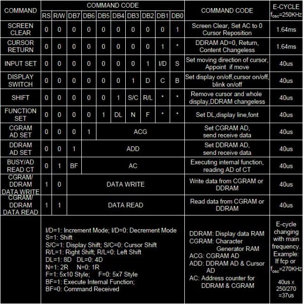
VIC has plenty of registers. Most of the registers that are used to configure interrupts or read status have each bit corresponding to a particular interrupt source and this mapping is same for all of these registers. What I mean is that bit 0 in these registers corresponds to Watch dog timer interrupt , bit 4 corresponds to TIMER0 interrupt , bit 6 corresponds to UART0 interrupt .. and so on.

Here is the complete table which says which bit corresponds to which interrupt source as given in Datasheet:

Table 1:
Bit# 22 21 20 19 18 17 16 15 14 13 12 11
IRQ USB AD1 BOD I2C1 AD0 EINT3 EINT2 EINT1 EINT0 RTC PLL SPI1/SSP
Bit# 10 9 8 7 6 5 4 3 2 1 0
IRQ SPI0 I2C0 PWM UART1 UART0 TIMR1 TIMR0 ARMC1 ARMC0 N/A WDT

Note : TIMR0 = TIMER0 , TIMR1 = TIMER1 , ARMC1 = ARMCore1 , ARMC2 = ARMCore2.

LPC2148 Interrupt Related Registers

Now we will have a look at some of the important Registers that are used to implement interrupts in lpc214x:

1) VICIntSelect (R/W) :

This register is used to select an interrupt as IRQ or as FIQ. Writing a 0 at a given bit location(as given in Table 1) will make the corresponding interrupt as IRQ and writing a 1 will make it FIQ. For e.g if you make Bit 4 as 0 then the corresponding interrupt source i.e TIMER0 will be IRQ else if you make Bit 4 as 1 it will be FIQ instead. Note than by default all interrupts are selected as IRQ. Note that here IRQ applies for both Vectored and Non-Vectored IRQs. [Refer Table 1]

2) VICIntEnable (R/W) :

This is used to enable interrupts. Writing a 1 at a given bit location will make the corresponding interrupt Enabled. If this register is read then 1′s will indicated enabled interrupts and 0′s as disabled interrupts. Writing 0′s has no effect. [Refer Table 1]

3) VICIntEnClr (R/W) :

This register is used to disable interrupts. This is similar to VICIntEnable expect writing a 1 here will disabled the corresponding Interrupt. This has an effect on VICIntEnable since writing at bit given location will clear the corresponding bit in the VICIntEnable Register. Writing 0′s has no effect. [Refer Table 1]

4) VICIRQStatus (R) :

This register is used for reading the current status of the enabled IRQ interrupts. If a bit location is read as 1 then it means that the corresponding interrupt is enabled and active. Reading a 0 is unless here lol.. [Refer Table 1]

5) VICFIQStatus (R) :

Same as VICIRQStatus except it applies for FIQ. [Refer Table 1]

6) VICSoftInt :

This register is used to generate interrupts using software i.e manually generating interrupts using code i.e the program itself. If you write a 1 at any bit location then the correspoding interrupt is triggered i.e. it forces the interrupt to occur. Writing 0 here has no effect. [Refer Table 1]

7) VICSoftIntClear :

This register is used to clear the interrupt request that was triggered(forced) using VICSoftInt. Writing a 1 will release(or clear) the forcing of the corresponding interrupt. [Refer Table 1]

8) VICVectCntl0 to VICVectCntl15 (16 registers in all) :

These are the Vector Control registers. These are used to assign a particular interrupt source to a particular slot. As mentioned before slot 0 i.e VICVectCntl0 has highest priority and VICVectCntl15 has the lowest. Each of this registers can be divided into 3 parts : {Bit0 to bit4} , {Bit 5} , {and rest of the bits}.

The first 5 bits i.e Bit 0 to Bit 4 contain the number of the interrupt request which is assigned to this slot. The interrupt source numbers are given in the table below :

Table 2:
Interrupt Source Source number
In Decimal
Interrupt Source Source number
In Decimal
WDT 0 PLL 12
N/A 1 RTC 13
ARMCore0 2 EINT0 14
ARMCore1 3 EINT1 15
TIMER0 4 EINT2 16
TIMER1 5 EINT3 17
UART0 6 ADC0 18
UART1 7 I2C1 19
PWM 8 BOD 20
I2C0 9 ADC1 21
SPI0 10 USB 22
SPI1 11

The 5th bit is used to enable the vectored IRQ slot by writing a 1.

Attention! : Note that if the vectored IRQ slot is disabled it will not disable the interrupt but will change the corresponding interrupt to Non-Vectored IRQ. Enabling the slot here means that it can generate the address of the ‘dedicated Interrupt handling function (ISR)’ and disabling it will generate the address of the ‘common/default Interrupt handling function (ISR)’ which is for Non-Vectored ISR. In simple words if the slot is enabled it points to ‘specific and dedicated interrupt handling function’ and if its disable it will point to the ‘default function’. This will get more clear as we do some examples.

Note : The Interrupt Source Number is also called as VIC Channel Mask. For this tutorial I’ll be calling it as “Interrupt Source Number” to keep things simple and clear. (^_^)

The rest of the bits are reserved.

9) VICVectAddr0 to VICVectAddr15 (16 registers in all) :

For Vectored IRQs these register store the address of the function that must be called when an interrupt occurs. Note – If you assign slot 3 for TIMER0 IRQ then care must be taken that you assign the address of the interrupt function to corresponding address register .. i.e VICVectAddr3 in this example.

10) VICVectAddr :

This must not be confused with the above set of 16 VICVecAddrX registers. When an interrupt is Triggered this register holds the address of the associated ISR i.e the one which is currently active. Writing a value i.e dummy write to this register indicates to the VIC that current Interrupt has finished execution. In this tutorial the only place we’ll use this register .. is at the end of the ISR to signal end of ISR execution.

11) VICDefVectAddr :

This register stores the address of the “default/common” ISR that must be called when a Non-Vectored IRQ occurs.

Now , that we’ve seen all the Registers , lets consider another Example with a Simple Diagram : Here we have 4 IRQs Configured. TIMER0 and SPI0 are configured as Vectored IRQs with TIMER0 having Highest Priority. UART0 and PWM IRQs are setup as Non-Vectored IRQs. The whole setup is as given below:

Configuring and Programming Interrupts (ISR)

To explain How to configure Interrupts and define ISRs I’ll use Timers as an example , since this Timers are easy to play. Hence , I Assume you are comfortable with using timers with LPC214x ;) .

First lets see how to define the ISR so that compiler handles it carefully. For this we need to explicitly tell the compiler that the function is not a normal function but an ISR. For this we’ll use a special keyword called “__irq” which is a function qualifier. If you use this keyword with the function definition then compiler will automatically treat it as an ISR. Here is an example on how to define an ISR in Keil :

__irq void myISR (void)
{
 ...
}

//====OR Equivalently====

void myISR (void) __irq
{
 ...
}

Note that both are perfectly valid ways of defining the ISR. I prefer to use __irq before the function name.

Now lets see how to actually setup the interrupt. Consider we wanna assign TIMER0 IRQ and ISR to slot X. Here is a simple procedure like thing to do that :

A Simple 3 Step Process to Setup / Enable a Vectored IRQ

  1. First we need to enable the TIMER0 IRQ itself! Hence , from Table 1 we get the bit number to Enable TIMER0 Interrupt which is Bit number 4. Hence we must make bit 4 in VICVectEnable to ’1′.
  2. Next , from Table 2 we get the interrupt source number for TIMER0 which is decimal 4 and OR it with (1<<5) [i.e 5th bit=1 which enables the slot] and assign it to VICVectCntlX.
  3. Next assign the address of the related ISR to VICVectAddrX.

Here is a simple Template to do it:

Replace Y by the slot number you want then Replace X by the Interrupt Source Number as given in Table 2 and finally replace myISR with your own ISR’s function Name .. and you’r Done!

VICVectEnable |= (1<<Y) ;
VICVectCntlX = (1<<5) | Y ;
VICVectAddrX = (unsigned) myISR;

Using above steps we can Assign TIMER0 Interrupt to Slot number say.. 0 as follows :

VICVectEnable |= (1<<4) ; // Enable TIMER0 IRQ
VICVectCntl0 = (1<<5) | 4 ; //5th bit must 1 to enable the slot (see the register definition above)
VICVectAddr0 = (unsigned) myISR;
//Vectored-IRQ for TIMER0 has been configured

Attention! : Note the Correspondence between the Bit number in Table 1 and the Source Number in Table 2. The Bit Number now becomes the Source Number in decimal.

Having done that now its time to write the code for the ISR.

More Attention plz! : First thing to note here is that each device(or block) in lpc214x has only 1 IRQ associated with it. But inside each device there may be different sources which can raise an interrupt (or an IRQ). Like the TIMER0 block(or device) has 4 match + 4 capture registers and any one or more of them can be configured to trigger an interrupt. Hence such devices have a dedicated interrupt register which contains a flag bit for each of these source(For Timer block its ‘T0IR‘). So , when the ISR is called first we need to identify the actual source of the interrupt using the Interrupt Register and then proceed accordingly. Also just before , when the main ISR code is finished we also need to acknowledge or signal that the ISR has finished executing for the current IRQ which triggered it. This is done by clearing the the flag(i.e the particular bit) in the device’s interrupt register and then by writing a zero to VICVectAddr register which signifies that interrupt has ISR has finished execution successfully.

Programming the Interrupt Service Routine (ISR) :

Okay to keep things keep simple lets consider two simple cases for coding an ISR (I’ll use TIMER0 for generating IRQs since its easy to understand and play with) :

  • Case #1) First when we have only one ‘internal’ source of interrupt in TIMER0 i.e an MR0 match event which raises an IRQ.
  • Case #2) And when we have multiple ‘internal’ source of interrupt in TIMER0 i.e. say a match event for MR0 , MR1 & MR2 which raise an IRQ.

In case #1 things are pretty straight forward. Since we know only one source is triggering an interrupt we don’t need to identify it – though its a good practice to explicitly identify it. The ISR then will be something like :

__irq void myISR(void)
{
    long int regVal;
    regVal = T0IR; // read the current value in T0's Interrupt Register
   
    //... MR0 match event has occured .. do something here
   
    T0IR = regval; // write back to clear the interrupt flag
    VICVectAddr = 0x0; // The ISR has finished!
}

Even in case #2 things are simple except we need to identify the ‘actual’ source of interrupt.

#define MR0I_FLAG (1<<0)
#define MR1I_FLAG (1<<1)
#define MR2I_FLAG (1<<2)

__irq void myISR(void)
{
    long int regVal;
    regVal = T0IR; // read the current value in T0's Interrupt Register
   
    if( T0IR & MR0I_FLAG )
    {
        //do something for MR0 match
    }
    else if ( T0IR & MR1I_FLAG )
    {
        //do something for MR1 match
    }
    else if ( T0IR & MR2I_FLAG )
    {
        //do something for MR2 match
    }
   
    T0IR = regVal; // write back to clear the interrupt flag
    VICVectAddr = 0x0; // Acknowledge that ISR has finished execution
}

Okay… Did you Notice a Second use of Case #2 ? If not then here it is .. : Case #2 actually provides a general method of using Timers as PWM generators! You can use any one of the match registers as PWM Cycle generator and then use other 3 match registers to generate 3 PWM signals! Since LPC214x already has PWM generator blocks on chip I don’t see any use of Timers being used as PWM generators. But for MCUs which don’t have PWM generator blocks this is very useful.

Soo , Now its time to go one step further and pop-out Case #3 and Case #4 out of the blue :P . Both of them deal with IRQs from different blocks viz. TIMER0 and UART0.

  • Case #3) When we have Multiple Vectored IRQs from different Devices. Hence Priority comes into picture here.
  • Case #4) Lastly when we have Multiple Non-Vectored IRQs from different Devices.

Don’t worry if your not acquianted with with UARTs , I’ll be Posting a Tutorial on UART with LPC214x shortly – Its in the pipeline :) .

For Case #3 , Consider we have TIMER0 and UART0 generating interrupts with TIMER0 having higher priority. So in this case we’ll need to write 2 different Vectored ISRs – one for TIMER0 and one for UART0. To keep things simple lets assume that we have only 1 internal source inside both TIMER0 and UART0 which generates an interrupt. The ISRs will be something as given below :

__irq void myTimer0_ISR(void)
{
    //Same as in case #1
}

__irq void myUart0_ISR(void)
{
    long int regVal;
    regVal = U0IIR; // read the current value in U0's Interrupt Register
                // which also clears it!
   
    //Something inside UART0 has raised an IRQ
   
    VICVectAddr = 0x0; // The ISR has finished!
}

For Case #4 too we have TIMER0 and UART0 generating interrupts. But here both of them are Non-Vectored and hence will be serviced by a common Non-Vectored ISR. Hence, here we will need to check the actual source i.e device which triggered the interrupt and proceed accordingly. This is quite similar to Case #2. The default ISR in this case will be something like :

__irq void myDefault_ISR(void)
{
    long int T0RegVal , U0RegVal;
    T0RegVal = T0IR; // read the current value in T0's Interrupt Register
    U0RegVal = U0IIR; // read the current value in U0's(Uart 0) Interrupt Identification Register
   
    if( T0IR )
    {
        //do something for TIMER0 Interrupt
       
        T0IR = T0RegVal; // write back to clear the interrupt flag for T0
    }
   
    if( ! (U0RegVal & 0x1) )
    {
        //do something for UART0 Interrupt
        //No need to write back to U0IIR since reading it clears it
    }
     
    VICVectAddr = 0x0; // The ISR has finished!
}

Attention Plz!: Note than UART0′s Interrupt Register is a lot different than TIMER0′s. The first Bit in U0IIR indicates whether any interrupt is pending or not and its Active LOW! The next 3 bits give the Identification for any of the 4 Interrupts if enabled. There is more to it which I’ll explain in detail in Upcoming Dedicated Tutorial on Uarts and Interrupt Programming related to it.

But Wait! What about FIQ ?

Well , you can think FIQ as a promoted version of a Vectored IRQ. To promote or covert a Vectored IRQ to FIQ just make the bit for corresponding IRQ in VICIntSelect register to 1 and it will be become an FIQ. [Refer Table 1] Also Note that its recommended that you only have one FIQ in your system. FIQs have low latency than VIRQs and usually used in System Critical Interrupt Handling.

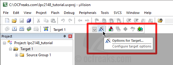
In Case Interrupts are Not working in Keil UV4 / Crossworks :

For those of you who are using Keil UV Version4(or higher) you’ll need to edit Target Option settings and those who are using Crossworks for ARM etc .. you need to manually enable global interrupt. I’ve posted a solution for this @ http://www.ocfreaks.com/lpc2148-interrupt-problem-issue-fix. Please go through that post to make Interrupts work.

Example Source for all Cases:

Example 1 – for Case #1:

For 1st example I’ll cover an interrupt driven ‘blinky’ using timers which I’ve also use in the LPC214x Timer Tutorial which can be found here : http://www.ocfreaks.com/lpc2148-timer-tutorial/ You can get the Complete Source and KeilUV4 Project files from the given link itself. Here is a snippet of the code for Case #1:

/*
(C) Umang Gajera | Power_user_EX - www.ocfreaks.com 2011-13.
More Embedded tutorials @ www.ocfreaks.com/cat/embedded

Soruce for Interrupt Tutorial Case #1.
License : GPL.
*/


#include <lpc214x.h>

#define MR0I (1<<0) //Interrupt When TC matches MR0
#define MR0R (1<<1) //Reset TC when TC matches MR0

#define DELAY_MS 500 //0.5 Second(s) Delay
#define PRESCALE 60000 //60000 PCLK clock cycles to increment TC by 1

void initClocks(void);
void initTimer0(void);
__irq void T0ISR(void);
void initClocks(void);

int main(void)
{
    initClocks(); //Initialize CPU and Peripheral Clocks @ 60Mhz
    initTimer0(); //Initialize Timer0
    IO0DIR = 0xFFFFFFFF; //Configure all pins on Port 0 as Output
    IO0PIN = 0x0;
   
    T0TCR = 0x01; //Enable timer

    while(1); //Infinite Idle Loop

    //return 0; //normally this wont execute ever   :P
}

void initTimer0(void)
{
    /*Assuming that PLL0 has been setup with CCLK = 60Mhz and PCLK also = 60Mhz.*/
   
    //----------Configure Timer0-------------

    T0CTCR = 0x0;                                      
   
    T0PR = PRESCALE-1; //(Value in Decimal!) - Increment T0TC at every 60000 clock cycles
                     //Count begins from zero hence subtracting 1
                     //60000 clock cycles @60Mhz = 1 mS
   
    T0MR0 = DELAY_MS-1; //(Value in Decimal!) Zero Indexed Count - hence subtracting 1
   
    T0MCR = MR0I | MR0R; //Set bit0 & bit1 to High which is to : Interrupt & Reset TC on MR0  

    //----------Setup Timer0 Interrupt-------------

    VICVectAddr4 = (unsigned )T0ISR; //Pointer Interrupt Function (ISR)

    VICVectCntl4 = 0x20 | 4; //0x20 (i.e bit5 = 1) -> to enable Vectored IRQ slot
                  //0x4 (bit[4:0]) -> this the source number - here its timer0 which has VIC channel mask # as 4
                  //You can get the VIC Channel number from Lpc214x manual R2 - pg 58 / sec 5.5
   
    VICIntEnable = 0x10; //Enable timer0 int
   
    T0TCR = 0x02; //Reset Timer
}

__irq void T0ISR(void)
{
    long int regVal;
    regVal = T0IR; //Read current IR value
       
    IO0PIN = ~IO0PIN; //Toggle all pins in Port 0

    T0IR = regVal; //Write back to IR to clear Interrupt Flag
    VICVectAddr = 0x0; //This is to signal end of interrupt execution
}

void initClocks(void)
{
  // This function is used to config PPL0 and setup both
  // CPU and Peripheral clock @ 60Mhz
  // You can find its definition in the attached files or case #2 source  
}

Download Project Source for Case #1 @ OCFreaks.com_LPC214x_TimerIRQ_Tutorial.zip [Successfully tested on Keil UV4.70a]

Example 2 – for Case #2:

This is an extended version of blinky which uses 3 Match Registers i.e 3 Interrupts sources within TIMER0 itself. Each Match register Interrupt is used to Turn on and off an LED which is connected to a particular GPIO Pin. Here we have 3 LEDs connected to PIN0 , PIN1 and PIN2 of PORT0 of LPC2148. MR0 is used for PIN0 i.e first LED , similarly MR2 and MR3 for PIN1 and PIN2 i.e for second and thrid LED respectively. MR0 has been configured to Trigger an Interrupt when 500ms have elapsed after TC is reset. MR1 has been configured to Trigger an Interrupt when 1000ms have elapsed after TC is reset. MR2 has been configured to Trigger an Interrupt when 1500ms have elapsed at it Resets the TC so the cycle starts again. Given a period of 1.5 seconds i.e 1500ms here is what happens :

1) MR0 Toggles PIN0 of PORT0 i.e P0.0 at 500ms
2) MR1 Toggles PIN1 of PORT0 i.e P0.1 at 1000ms
3) MR2 Toggles PIN2 of PORT0 i.e P0.2 at 1500ms and also Resets the TC
*) This cycle of Toggling each of the LEDs one by one keeps on repeating…

/*
(C) Umang Gajera | Power_user_EX - www.ocfreaks.com 2011-13.
More Embedded tutorials @ www.ocfreaks.com/cat/embedded

LPC2148 Interrupt Example.
License : GPL.
*/


#include <lpc214x.h>

#define PLOCK 0x00000400
#define MR0I (1<<0) //Interrupt When TC matches MR0
#define MR1I (1<<3) //Interrupt When TC matches MR1
#define MR2I (1<<6) //Interrupt When TC matches MR2
#define MR2R (1<<7) //Reset TC when TC matches MR2

#define MR0I_FLAG (1<<0) //Interrupt Flag for MR0
#define MR1I_FLAG (1<<1) //Interrupt Flag for MR1
#define MR2I_FLAG (1<<2) //Interrupt Flag for MR2

#define MR0_DELAY_MS 500 //0.5 Second(s) Delay
#define MR1_DELAY_MS 1000 //1 Second Delay
#define MR2_DELAY_MS 1500 //1.5 Second(s) Delay
#define PRESCALE 60000 //60000 PCLK clock cycles to increment TC by 1

void delayMS(unsigned int milliseconds);
void initClocks(void);
void initTimer0(void);
__irq void myTimer0_ISR(void);

void setupPLL0(void);
void feedSeq(void);
void connectPLL0(void);


int main(void)
{
    initClocks(); //Initialize CPU and Peripheral Clocks @ 60Mhz
    initTimer0(); //Initialize Timer0
    IO0DIR = 0xFFFFFFFF; //Configure all pins on Port 0 as Output
    IO0PIN = 0x0;
   
    T0TCR = 0x01; //Enable timer

    while(1); //Infinite Idle Loop

    //return 0; //normally this wont execute ever   :P
}

void initTimer0(void)
{
    /*Assuming that PLL0 has been setup with CCLK = 60Mhz and PCLK also = 60Mhz.*/
   
    //----------Configure Timer0-------------

    T0CTCR = 0x0;  
   
    T0PR = PRESCALE-1; //60000 clock cycles @60Mhz = 1 mS
   
    T0MR0 = MR0_DELAY_MS-1; // 0.5sec (Value in Decimal!) Zero Indexed Count - hence subtracting 1

    T0MR1 = MR1_DELAY_MS-1; // 1sec

    T0MR2 = MR2_DELAY_MS-1; // 1.5secs
   
    T0MCR = MR0I | MR1I | MR2I | MR2R; //Set the Match control register

    //----------Setup Timer0 Interrupt-------------

    //I've just randomly picked-up slot 4

    VICVectAddr4 = (unsigned)myTimer0_ISR; //Pointer Interrupt Function (ISR)

    VICVectCntl4 = 0x20 | 4;

    VICIntEnable = 0x10; //Enable timer0 int
   
    T0TCR = 0x02; //Reset Timer
}

__irq void myTimer0_ISR(void)
{
    long int regVal;
    regVal = T0IR; // read the current value in T0's Interrupt Register

    if( T0IR & MR0I_FLAG )
    {
        //do something for MR0 match

        IO0PIN ^= (1<<0); // Toggle GPIO0 PIN0 .. P0.0
   
    }
    else if ( T0IR & MR1I_FLAG )
    {
        //do something for MR1 match
       
        IO0PIN ^= (1<<1);// Toggle GPIO0 PIN1 .. P0.1
   
    }
    else if ( T0IR & MR2I_FLAG )
    {
        //do something for MR0 match
       
        IO0PIN ^= (1<<2);// Toggle GPIO0 PIN2 .. P0.2
   
    }
   
    T0IR = regVal; // write back to clear the interrupt flag
    VICVectAddr = 0x0; // Acknowledge that ISR has finished execution
}

void initClocks(void)
{
    setupPLL0();
    feedSeq(); //sequence for locking PLL to desired freq.
    connectPLL0();
    feedSeq(); //sequence for connecting the PLL as system clock
   
    //SysClock is now ticking @ 60Mhz!
       
    VPBDIV = 0x01; // PCLK is same as CCLK i.e 60Mhz

    //PLL0 Now configured!
}

//---------PLL Related Functions :---------------

//Using PLL settings as shown in : http://www.ocfreaks.com/lpc214x-pll-tutorial-for-cpu-and-peripheral-clock/

void setupPLL0(void)
{
    //Note : Assuming 12Mhz Xtal is connected to LPC2148.
   
    PLL0CON = 0x01;
    PLL0CFG = 0x24;
}

void feedSeq(void)
{
    PLL0FEED = 0xAA;
    PLL0FEED = 0x55;
}

void connectPLL0(void)
{
    while( !( PLL0STAT & PLOCK ));
    PLL0CON = 0x03;
}

Note: TC is reset only when MR2 matches TC. Though this can be used using simple delay but the example presented here does this by purely using Interrupts!

Download Project Source for Case #2 @ OCFreaks.com_LPC214x_Interrupt_Tutorial_Case2.zip [Successfully tested on Keil UV4.70a]

Example 3 – for Case #3:

Note that Case #3 and Case #4 are just some Fictitious-Typo cases which I’ve randomly made to Explain Multiple Vectored and Non-Vectored IRQs. I haven’t tried them out on my Development Board yet , but since the Simulation seems to work perfect I assume both will work as expected if you try them out. If any doesn’t work please let me know.

Consider we have TIMER0 generating interrupt every 500ms and UART0 generates an interrupt when some data arrives i.e when you press a key in the terminal. TIMER0 ISR will Toggle P0.2 and UART0 ISR will Toggle P0.3. Here TIMER0 ISR will have a higher priority over UART0 ISR. Hence when TIMER0 interrupt occurs and at the same time UART0 interrupt occurs , first TIMER0 ISR will be serviced and then UART0.

Here I’m only giving the code to Enable both the Interrupts and its ISR. You can find the complete code in files attached below.

Code for Configuring Both TIMER0 and UART0 Interrupts is as given Below:

//----------Setup TIMER0 Interrupt-------------

//Using Slot 0 for TIMER0

VICVectAddr0 = (unsigned)myTimer0_ISR; //Pointer Interrupt Function (ISR)

VICVectCntl0 = 0x20 | 4;

VICIntEnable |= (1<<4); //Enable timer0 int , 4th bit=1

//----------Setup UART0 Interrupt-------------

//Any Slot with Lower Priority than TIMER0's slot will suffice

VICVectAddr1 = (unsigned)myUart0_ISR; //Pointer Interrupt Function (ISR)

VICVectCntl1 = 0x20 | 6;

VICIntEnable |= (1<<6); //Enable Uart0 interrupt , 6th bit=1

Both the ISRs will be as follows :

__irq void myTimer0_ISR(void)
{
    long int regVal;
    regVal = T0IR; // read the current value in T0's Interrupt Register
   
    IO0PIN ^= (1<<2); // Toggle 3rd Pin in GPIO0 .. P0.2

    T0IR = regVal; // write back to clear the interrupt flag
    VICVectAddr = 0x0; // Acknowledge that ISR has finished execution
}

__irq void myUart0_ISR(void)
{
    long int regVal;
    regVal = U0IIR; // Reading U0IIR also clears it!
   
    //Recieve Data Available Interrupt has occured
    regVal = U0RBR; // dummy read
    IO0PIN ^= (1<<3); // Toggle 4th Pin in GPIO0 .. P0.3

    VICVectAddr = 0x0; // Acknowledge that ISR has finished execution
}

Download Project Source for Case #3 @ OCFreaks.com_LPC214x_Interrupt_Tutorial_Case3.zip [Successfully tested on Keil UV4.70a]

Example 4 – for Case #4:

Even Here I’ll give the main code and as with above you can find the complete code in the attached files.

In the Non-Vectored Case the configuration code will be as shown below:

VICDefVectAddr = (unsigned)myDefault_ISR; //Pointer to Default ISR

//----------Enable (Non-Vectored) TIMER0 Interrupt-------------

VICIntEnable |= (1<<4); //Enable timer0 int , 4th bit=1

//----------Enable (Non-Vectored) UART0 Interrupt-------------

VICIntEnable |= (1<<6); //Enable Uart0 interrupt , 6th bit=1

And the code for the Non-Vectored ISR is as given Below:

__irq void myDefault_ISR(void)
{
    long int T0RegVal , U0RegVal;
    T0RegVal = T0IR; // read the current value in T0's Interrupt Register
    U0RegVal = U0IIR;
   
    if( T0IR )
    {
        IO0PIN ^= (1<<2); // Toggle 3rd Pin in GPIO0 .. P0.2
        T0IR = T0RegVal; // write back to clear the interrupt flag
    }
   
    if( !(U0RegVal & 0x1) )
    {
        //Recieve Data Available Interrupt has occured
        U0RegVal = U0RBR; // dummy read
        IO0PIN ^= (1<<3); // Toggle 4th Pin in GPIO0 .. P0.3
    }
   
    VICVectAddr = 0x0; // Acknowledge that ISR has finished execution
}

Download Project Source for Case #4 @ OCFreaks.com_LPC214x_Interrupt_Tutorial_Case4.zip [Successfully tested on Keil UV4.70a]
FINAL Attention Plz! : When you play with Multiple Interrupts , Please take care of all the situations that may arise else in most cases Weird System Behavior might creep in giving you Debugging Nightmares. I’d say keep on experimenting with Interrupts .. the more you’ll do the more you’ll learn and the more clear it will become!

Advanced Interrupt Handling:

Nested Interrupts:

Interrupts too can be nested. But we need to take some special care when dealing with nested interrupts since in this case the “context” and the “stack” come into picture. When a nested interrupt has finished execution we must get back to the correct context. Similarly too much of nesting and the stack will get overloaded. Covering Nested interrupt is not within the scope of this tutorial. Here are some useful documents which will surely help you out with interrupt nesting.

For more on Nested Interrupts you can refer the following documents :

  1. NXP Application Note : AN10381
  2. http://www.keil.com/support/docs/3353.htm

Spurious Interrupts:

I like to call “Spurious Interrupt” as “Zombie Interrupts:D – in my opinion that suits it more. These can happen in virtually any interrupt driven system and must be identified and handled properly else undefined system behaviour may occur. Such interrupts happen when an IRQ is generated out of no where (Magic! lol..). Here the IRQ comes into exsistence even when none of the conditions for triggering that IRQ have been met. Normally speaking its an interrupt that was not required in the first place. There are many reasons as to why it can happen :

  • 1) Inherent bug/flaw in system design
  • 2) Electrical Interference / Noise
  • 3) Software Bug
  • 4) Signal glitches on Level Sensitive interrupts
  • 5) Faulty components
  • 6) Misconfigured Hardware
  • 7) etc… (You’ll get plently of info just by googling the term)

In respect to LPC214x(also LPC2000) MCUs , the probability of occurrence of Spurious Interrupts is high when Watch Dog Timer or UART is used. The datasheet(manual) has special note on Spurious interrupts on page 61. Covering the “handling of Spurious Interrupts” is too not in the scope of this article.

For more information on handling of spurious interrupts I would like my readers to go through the following documents :

  1. Page 61 of LPC214x Usermanul Rev 2.0
  2. NXP Application Note : AN10414

Understanding VIC in Detail:

Finally , I’d like to share one of the best guide I’ve found for Understanding the general Architecture of VIC in detail .. which is the following document from ARM itself :

  1. http://infocenter.arm.com/help/topic/com.arm.doc.ddi0181e/DDI0181.pdf

Related posts:

  1. LPC2148 Interrupt Problem and Issue fix
  2. LPC2148 Timer Tutorial
  3. LPC2148 GPIO Programming Tutorial

Pulse Width Modulation (PWM) Tutorial

$
0
0

Pulse Width Modulation Basics

Pulse Width Modulation or PWM is a way to encode data such that it corresponds to the width of the pulse given a fixed frequency. Its also a way to control motors , power circuits , etc.. using the ‘width’ of the pulse. PWM has numerous uses like Motion Control , Dimming , Encoding Analog Signal into its Digital form , in Power Regulation , etc.

Period(T) & PWM Frequency :

Period(T) can be thought of as the Time required for a new pulse to arrive – its basically the sum of ON time(T-ON) and OFF time(T-OFF) of a PWM cycle. PWM Frequency is the rate at which a PWM pulse is repeated. It can be also called as the “Repetition Rate”. Frequency is the inverse of the Period. PWM Frequency is fixed Depending on the application. As a simple example lets consider a RC Servo Motor. This type of Servos expect a new Pulse every 20ms which is the Period. Hence in this case the PWM frequency is 1/20ms = 50hz.

T-ON , T-OFF & DutyCycle :

Each Period of PWM signal is divided into T-ON and T-OFF. Where T-ON is the Time required or taken for the pulse to remain ON i.e in a HIGH state and similarly T-OFF is the Time required or taken for the pulse to remain OFF i.e in a LOW state. Now , the DUTY-CYCLE is the percentage of period required for T-ON. For example if T-ON=T-OFF then the period is divided into 2 equal parts i.e 50(TON):50(TOFF). Hence the DUTY-CYCLE will be 50%. If T-OFF is 3 Times T-ON then period is divided into 2 unequal Parts i.e 25(TON):75(TOFF) .. hence DUTY-CYCLE in this case will be 25%. DutyCycle can be expressed as a simple formula given below:

Duty Cycle as a Ratio:
Duty Cycle =   T-ON
T-ON + T-OFF

DutyCycle in Percentage is :

Duty Cycle % =   T-ON x 100
T-ON + T-OFF

Example :

In PWM diagram shown above we have ,

Period i.e T = 10ms
Hence , Frequency = 100hz

T-ON = 3.5ms
T-OFF = 6.5ms

Hence , DutyCyle = 35%

PWM Edges

A PWM signal contains 2 types of Edges which are called Leading Edge and Trailing Edge. The Diagram shown below explains this:

Types of PWM

PWM Signal can be Classified in Different ways. However , I would like to classify PWM as :

1) Single Edge PWM
2) Double Edge PWM

Single Edge PWM

Single Edge PWM the Pulse can either at the Beginning or the End of the Period and hence can be further Classified into Leading Edge(Right Aligned) PWM and Trailing Edge(Left Aligned) PWM.

In Trailing Edge PWM the Leading Edge is fixed at the Beginning of a Period and the Trailing Edge is Modulated i.e. Varied. Diagram for Trailing Edge(Left Aligned) PWM:

In Leading Edge PWM the Trailing Edge is fixed at the End of a Period and the Leading Edge is Modulated i.e. Varied. Diagram for Leading Edge(Right Aligned) PWM:

Double Edge PWM

In Double Edge PWM the Pulse can be Positioned anywhere within the Period. Its called “Double Edge” because both the Edges are Modulated or Varied. In applications like Multi-Phase Motor control Double Edge PWM is used where the Pulse is Center Aligned to reduce Harmonics. Diagram for Double Edge Center Aligned PWM is as shown below:

PWM Voltage

The Average Voltage of a PWM Output depends on its Duty Cycle. Lower the Duty Cycle lower will be the Voltage and Vice-Verse. The maximum Voltage will be equal to the Value of the High State and the minimum Voltage will be equal to Low state of the Pulse. For e.g. if High state is 5V and Low state is 0v the maximum Voltage will be 5V at 100% duty cycle and min Voltage will be 0V at 0% duty cycle.

Vaverage = DutyCycle x VH

In case the Low State Represents a Negative Voltage then the above equation can be generalized as follows :

Vaverage = (DutyCycle x VH) + ((1-D) x VL)

Where , VH = Voltage for High State & VL = Voltage for Low State

This can be converted into an Analog Voltage by Using a Simple R-C filter.

Note : This Tutorial is a supplementary material for tutorials on PWM generation using MCUs like LPC176x , LPC214x , etc..

Related posts:

  1. LPC2148 Timer Tutorial
  2. Interfacing 16X2 LCD with LPC2148 tutorial

LPC2148 PWM Programming Tutorial

$
0
0

Introduction

This Tutorial is for learning Pulse Width Modulation (PWM) programming for LPC214x MCUs. For this Tutorial I’ll be covering Single Edge PWM and how to use to control Motors like Servos. Also for the scope of this tutorial I won’t be going into stuff like MCU controlled Voltage Regulation using PWM since I am planning a dedicated tutorial for that. I assume you are comfortable with Timers and its usage in LPC214x since PWM block is basically a Timer. I’ve posted a tutorial on Timers in LPC214x @ Here – just in case if you need it.

Pulse Width Modulation Basics :

I’ve Posted a Beginner PWM tutorial @ Basic PWM Tutorial. If you are new to PWM please have a look there.

Here is Diagram that sums it up. It shows Single Edge PWM with T-ON , T-OFF & Period. Duty Cycle is simply T-ON Divided by Period.

PWM Programming in LPC2148

LPC2148 supports 2 types of PWM :
1) Single Edge PWM – Pulse starts with new Period i.e pulse is always at the beginning
2) Double Edge PWM – Pulse can be anywhere within the Period

A PWM block , like a Timer block , has a Timer Counter and an associated Prescale Register along with Match Registers. These work exactly the same way as in the case of Timers. I’ve explained them in the introduction part of the Lpc214x Timer tutorial @ Here . Match Registers 1 to 6 (except 0) are pinned on LPC214x i.e. the corresponding outputs are diverted to actual Pins on LPC214x MCU. The PWM function must be selected for these Pins to get the PWM output. These pins are :


Output : PWM1 PWM2 PWM3 PWM4 PWM5 PWM6
Pin Name : P0.0 P0.7 P0.1 P0.8 P0.21 P0.9

Note : PWM1 output corresponds to PWM Match Register 1 i.e PWMMR1 , PWM2 output corresponds to PWMMR2 , and so on. Also Match Register 0 i.e PWMMR0 is NOT pinned because it is used to generate the PWM Period. Also the PWM function must be selected for the PINs mentioned above using appropriate PINSEL registers (PINSEL0 for PWM1,2,3,4,6 and PINSEL1 for PWM5).

In LPC214x we have 7 match registers inside the PWM block . Generally the first Match register PWMMR0 is used to generate PWM period and hence we are left with 6 Match Registers PWMMR1 to PWMMR6 to generate 6 Single Edge PWM signals or 3 Double Edge PWM signals. Double edge PWM uses 2 match registers hence we can get only 3 double edge outputs. The way this works in case of Single Edge PWM is as follows (and similarly for Double Edge):

  1. Consider that our PWM Period duration is 6 milliseconds and TC increments every 1 millisecond using appropriate prescale value.
  2. Now we set the match value in PWMMR0 as 6 , Note : This period will be same for all PWM outputs!
  3. Then we configure PWM block such that when TC reaches value in PWMMR0 it is reset and a new Period begins.
  4. Now lets say we want 2 PWM signals of Pulse widths 2ms and 4ms.
  5. So .. we can use PWMMR1 and PWMMR2 to get the 2 outputs. For that we set PWMMR1 = 2 and PWMMR2 = 4.
  6. Then , Everytime a new period starts the Pin corresponding to PWMMR1 and PWMMR2 will be set High by default.
  7. And .. Whenever the value in TC reaches PWMMR1 and PWMMR2 its output will be set to low respectively.
  8. Their outputs will remain low until the next Period starts after which their outputs again become high .. hence giving us Single Edge PWM.

This can be shown in the diagram below:

PWM Rules : The LPC214x User Manual mentions Rules for using Single Edge and Double Edge PWM on page 261 . The Rules for Single Edged PWM are as :
  • 1) All single edged PWM outputs will go high at the beginning of a PWM cycle unless their match value is 0.
  • 2) Each PWM output will go low when its match value is reached. Note : If no match occurs i.e Match value is greater than Period then the output will remain high!

For Double Edge Rules you can refer the User Manual Pg. 261.

Note 1: The last 6 Match Registers i.e PWMMR1 to PWMMR6 have an associated PIN from which we get the PWM outputs. The PWM block controls the output of these pins depending on the value in its corresponding Match Register. For Single Edged PWM these Pins are set to High by default when a new Period starts i.e when TC is reset as per the PWM Rules given above.

Note 2: Note that Here we are storing the width of the Pulse in the Match Register. We can also change the width of the pulse by changing the value in the corresponding Match register using a special register called Latch Enable Register which is used to control the way Match Registers get updated. I’ll explain this shortly. First Lets see all the Registers in PWM Block in LPC2148.

Now lets have a look at some important Registers :

1) PWMTCR : PWM Timer Control Register

This register is used to control the Timer Counter inside the PWM block. Only Bits: 0, 1 & 3 are used rest are reserverd.

  • Bit 0 : This bit is used to Enable/Disable Counting. When 1 both PWM Timer counter and PWM Prescale counter are enabled. When 0 both are disabled.
  • Bit 1 : This bit is used to Reset both Timer and Prescale counter inside the PWM block. When set to 1 it will reset both of them (at next edge of PCLK).
  • Bit 3 : This is used to enable the PWM mode i.e the PWM outputs.
    Other Bits : Reserved.

2) PWMPR : PWM Prescale Register

PWMPR is used to control the resolution of the PWM outputs. The Timer Counter(TC) will increment every PWMPR+1 Peripheral Clock Cycles (PCLK).

3) PWMMR0 – PWMMR6 : Match Registers

These are the seven Match registers as explained above which contain Pulse Width Values i.e the Number of PWMTC Ticks.

4) PWMMCR : PWM Match Control Registers

The PWM Match Control Register is used to specify what operations can be done when the value in a particular Match register equals the value in TC. For each Match Register we have 3 options : Either generate an Interrupt , or Reset the TC , or Stop .. which stops the counters and disables PWM. Hence this register is divided into group of 3 bits. The first 3 bits are for Match Register 0 i.e PWMMR0 , next 3 for PWMMR1 , and so on :

  • 1) Bit 0 : Interrupt on PWMMR0 Match – If set to 1 then it will generate an Interrupt else disable if set to 0.
  • 2) Bit 1 : Reset on PWMMR0 Match – If set to 1 it will reset the Timer Counter i.e PWMTC else disabled if set to 0.
  • 3) Bit 2 : Stop on PWMMR0 Match – If this bit is set 1 then both PWMTC and PWMPC will be stopped and will also make Bit 0 in PWMTCR to 0 which in turn will disable the Counters.
  • *) Similarly {Bits 3,4,5} for PWMMR1 , {Bits 6,7,8} for PWMMR2 , {Bits 9,10,11} for PWMMR3 ,{Bits 12,13,14} for PWMMR4 ,{Bits 15,16,17} for PWMMR5 , {Bits 18,19,20} for PWMMR6.

5) PWMIR : PWM Interrupt Register

If an interrupt is generated by any of the Match Register then the corresponding bit in PWMIR will be set high. Writing a 1 to the corresponding location will clear that interrupt. Here :

  • 1) Bits 0,1,2,3 are for PWMMR0, PWMMR1, PWMMR2, PWMMR3 respectively and
  • 2) Bits 8,9,10 are for PWMMR4 , PWMMR5 , PWMMR6 respectively. Other bits are reserved.

6) PWMLER : Latch Enable Register

The PWM Latch Enable Register is used to control the way Match Registers are updated when PWM generation is active. When PWM mode is active and we apply new values to the Match Registers the new values won’t get applied immediately. Instead what happens is that the value is written to a “Shadow Register” .. it can be thought of as a duplicate Match Register. Each Match Register has a corresponding Shadow Register. The value in this Shadow Register is transferred to the actual Match Register when :

1) PWMTC is reset (i.e at the beginning of the next period) ,
2) And the corresponding Bit in PWMLER is 1.

Hence only when these 2 conditions are satisfied the value is copied to Match Register. Bit ‘x’ in PWMLER corresponds to match Register ‘x’. I.e Bit 0 is for PWMMR0 , Bit 1 for PWMMR1 , .. and so on. Using PWMLER will be covered in the examples section.

7) PWMPCR : PWM Control Register

This register is used for Selecting between Single Edged & Double Edged outputs and also to Enable/Disable the 6 PWM outputs which go to their corresponding Pins.

  • 1) Bits 2 to 6 are used to select between Single or Double Edge mode for PWM 2,3,4,5,6 outputs.
    1) Bit 2 : If set to 1 then PWM2(i.e the one corresponding to PWMMR2) output is double edged else if set 0 then its Single Edged.
    2) Similarly {Bits 3,4,5,6} for PWM3 , PWM4 , PWM5 , PWM6 respectively.
  • 2) Bits 9 to 14 are used to Enable/Disable PWM outputs
    1) Bit 9 : If set to 1 then PWM1 output is enabled , else disabled if set to 0.
    2)Similarly {Bit 10,11,12,13,14} for PWM2 , PWM3 , PWM4 , PWM5 , PWM6 respectively.

Configuring and Initializing PWM :

Configuring PWM is very much similar to Configuring Timer except , additionally , we need to enable the outputs and select PWM functions for the corresponding PIN on which output will be available. But first we need to do some basic Math Calculations for defining the Period time , the resolution using a prescale value and then Pulse Widths. For this First we need to define the resolution of out PWM signal. Here the PWM resolution which I mean is the minimum increment that can use to increase or decrease the pulse width. More smaller the increment more fine will be the resolution. This resolution is defined using an appropriate Prescale Value. The calculation for Prescale is the same which I had shown in the Timer Tutorial .. but here it is once again :

PWM Prescale (PWMPR) Calculations:

The delay or time required for ‘Y’ clock cycles of PCLK at ‘X’ MHz is given by :
Delay =  Y seconds
X * 106

When we take PR into consideration we get Y = PR+1. Now , consider that PCLK is running at 60Mhz then X=60. Hence if we use Y=60 i.e PR=59 then we get a delay of exact 1 micro-second(s).

So with PR=59 and PCLK @ 60Mhz our formula reduces to :

Delay =  59+1 seconds = 1 micro-seconds
60 * 106

Similarly when we set Y=60000 i.e PR = 59999 the delay will be 1 milli-second(s) :

Delay =  599999+1 seconds = 1 milli-second
60 * 106

This delay which is defined using Prescale will be the delay required for TC to increment by 1 i.e TC will increment every ‘PR+1′ “Peripheral” Clock Cycles (PCLK).

Now , After we’ve worked out the resolution we want .. we can now Set and Initialize the PWM device as per the following steps :
  1. Select the PWM function for the PIN on which you need the PWM output using PINSEL0/1 register.
  2. Select Single Edge or Double Edge Mode using PWMPCR. By default its Single Edge Mode.
  3. Assign the Calculated value to PR.
  4. Set the Value for PWM Period in PWMMR0.
  5. Set the Values for other Match Registers i.e the Pulse Widths.
  6. Set appropriate bit values in PWMMCR .. like for e.g. resetting PWMTC for PWMMR0 match and optionally generate interrupts if required
  7. Set Latch Enable Bits for the Match Registers that you’ve used. This is important!
  8. Then Enable PWM outputs using PWMPCR.
  9. Now Reset PWM Timer using PWMTCR.
  10. Finally .. Enable Timer Counter and PWM Mode using PWMTCR.

Example :

PINSEL0 = ... ; // Select PWM Function for used Pins
PWMPCR = ... ; // Select PWM type - By default its Single Edged
PWMPR = ... ; //assign calculated PR value
PWMMR0 = ... ; // Assign Period Duration
PWMMRx = ... ; // Assign pulse duration i.e widths for other Match Regs.. x=1 to 6
PWMMCR = (1<<1) | ... ; // Reset PWMTC on PWMMR0 match & Other conditions
PWMLER = (1<<1) | ... ; // update MR0 and other Match Registers
PWMPCR = ... ; // enable PWM outputs as required
PWMTCR = (1<<1) ; //Reset PWM TC & PR

//Now , the final moment - enable everything
PWMTCR = (1<<0) | (1<<3); // enable counters and PWM Mode
//Done!

Updating Match Registers i.e the Pulse Width

Once PWM is initialized then you can update any of the Match Registers at anytime using PWMLER. This can be done as follows :

PWMMR1 = 50; // Update Pulse Width
PWMLER = (1<<1); // set the corresponding bit to 1

When you want to update Multiple Match Registers then this can be done as follows :

PWMMR1 = 50;
PWMMR2 = 68;
PWMMR3 = 20;

PWMLER = (1<<1) | (1<<2) | (1<<3); // Update Latch Enable bit for all MRs together

Some Real World Examples

I’ll cover 2 examples using Single Edge PWM. These will be:
1) Controlling RC Servo
2) LED Dimming

To stay within the scope of this article I’m not including a bit involved stuff like “RC Servo Speed Control” and “DC Motor Speed Control”. I guess I’ll do it in a separate article.

Before we get into the Examples , I would like to mention a few words about a function named “initClocks()” which I’ve been using in all examples. This function basically configures PLL0 and Sets up CPU Clock at 60Mhz and Peripheral Clock also at 60Mhz. You can find the the source for initClocks() in the Attached Project Files. If you are not sure about how to configure PPL0 in LPC214x , you can find a simple tutorial Here.

Example #1) Simple RC Servo Control Using PWM :

Here we will use PWM1 output from Pin P0.0 to control a RC Servo Motor. We will also be using 4 tactile switches to bring the Servo at 4 different positions. P0.1 , P0.2 , P0.3 , P0.4 will be used to take the input. One end of the tactile switches will be connected to each of these Pins and other end will be connected to ground. Here we’ll also require external 5V-6V source to drive the servo. Servos can work with 3.3v voltage levels for input PWM signal , hence we just need to connect the MCU PWM Output to Servo PWM Input wire. The setup is as shown in the schematic below :

When the user will press P0.1 the Pulse width will be 1ms , and similarly when the user presses P0.2 , P0.3 , P0.4 the Pulse Width will change to 1.25ms , 1.5ms and 1.75ms respectively and hence Servo will change its position correspondingly.

Source for Example 1:

/*
(C) Umang Gajera | Power_user_EX - www.ocfreaks.com 2011-13.
More Embedded tutorials @ www.ocfreaks.com/cat/embedded

LPC2148 PWM Tutorial Example 1 - RC Servo Control using PWM.
License : GPL.
*/

#include <lpc214x.h>

#define PLOCK 0x00000400
#define PWMPRESCALE 60   //60 PCLK cycles to increment TC by 1 i.e 1 Micro-second

void initPWM(void);
void initClocks(void);

int main(void)
{
    initClocks(); //Initialize CPU and Peripheral Clocks @ 60Mhz
    initPWM(); //Initialize PWM

    //IO0DIR = 0x1; This is not needed!
    //Also by default all pins are configured as Inputs after MCU Reset.
   
    while(1)
    {
        if( !((IO0PIN) & (1<<1)) ) // Check P0.1
        {
            PWMMR1 = 1000;
            PWMLER = (1<<1); //Update Latch Enable bit for PWMMR1
        }
        else if( !((IO0PIN) & (1<<2)) ) // Check P0.2
        {
            PWMMR1 = 1250;
            PWMLER = (1<<1);
        }
        else if( !((IO0PIN) & (1<<3)) ) // Check P0.3
        {
            PWMMR1 = 1500;
            PWMLER = (1<<1);
        }
        else if( !((IO0PIN) & (1<<4)) ) // Check P0.4
        {
            PWMMR1 = 1750;
            PWMLER = (1<<1);
        }
    }
    //return 0; //normally this wont execute ever
}

void initPWM(void)
{
    /*Assuming that PLL0 has been setup with CCLK = 60Mhz and PCLK also = 60Mhz.*/
    /*This is a per the Setup & Init Sequence given in the tutorial*/

    PINSEL0 = (1<<1); // Select PWM1 output for Pin0.0
    PWMPCR = 0x0; //Select Single Edge PWM - by default its single Edged so this line can be removed
    PWMPR = PWMPRESCALE-1; // 1 micro-second resolution
    PWMMR0 = 20000; // 20ms = 20k us - period duration
    PWMMR1 = 1000; // 1ms - pulse duration i.e width
    PWMMCR = (1<<1); // Reset PWMTC on PWMMR0 match
    PWMLER = (1<<1) | (1<<0); // update MR0 and MR1
    PWMPCR = (1<<9); // enable PWM output
    PWMTCR = (1<<1) ; //Reset PWM TC & PR

    //Now , the final moment - enable everything
    PWMTCR = (1<<0) | (1<<3); // enable counters and PWM Mode

    //PWM Generation goes active now!!
    //Now you can get the PWM output at Pin P0.0!
}

Download Project Source for Example #1 @ LPC214x PWM Tutorial Example 1.zip [Successfully tested on Keil UV4.70a]

Example #2) LED Dimming using PWM :

The basic Setup here is same as in Example 1 except that here we replace Servo by a LED and we dont need external 5V source along with slightly modified Program. Here we’ll just need to connect the anode of LED to P0.0 and cathode to GND. In this example will use a period of 10ms. In this case the Pulse Widths Corresponding to the Switches connected to P0.1/2/3/4 will be 2.5ms/5ms/7.5ms/10ms respectively. As the Pulse Width Increases LED will keep on getting Brighter and the reverse will happen if Pulse Width is decreased.

Source for Example 2:

/*
(C) Umang Gajera | Power_user_EX - www.ocfreaks.com 2011-13.
More Embedded tutorials @ www.ocfreaks.com/cat/embedded

LPC2148 PWM Tutorial Example 2 - LED Dimming using PWM.
License : GPL.
*/

#include <lpc214x.h>

#define PLOCK 0x00000400
#define PWMPRESCALE 60   //60 PCLK cycles to increment TC by 1 i.e 1 Micro-second

void initPWM(void);
void initClocks(void);

int main(void)
{
    initClocks(); //Initialize CPU and Peripheral Clocks @ 60Mhz
    initPWM(); //Initialize PWM

    //IO0DIR = 0x1; This is not needed!
    //Also by default all pins are configured as Inputs after MCU Reset.
   
    while(1)
    {
        if( !((IO0PIN) & (1<<1)) ) // Check P0.1
        {
            PWMMR1 = 2500; //T-ON=25% , Hence 25% Bright
            PWMLER = (1<<1); //Update Latch Enable bit for PWMMR1
        }
        else if( !((IO0PIN) & (1<<2)) ) // Check P0.2
        {
            PWMMR1 = 5000; //50% Bright
            PWMLER = (1<<1);
        }
        else if( !((IO0PIN) & (1<<3)) ) // Check P0.3
        {
            PWMMR1 = 7500; //75% Bright
            PWMLER = (1<<1);
        }
        else if( !((IO0PIN) & (1<<4)) ) // Check P0.4
        {
            PWMMR1 = 10000; //100% Bright
            PWMLER = (1<<1);
        }
    }
    //return 0; //normally this wont execute ever
}

void initPWM(void)
{
    /*Assuming that PLL0 has been setup with CCLK = 60Mhz and PCLK also = 60Mhz.*/
    /*This is a per the Setup & Init Sequence given in the tutorial*/

    PINSEL0 = (1<<1); // Select PWM1 output for Pin0.0
    PWMPCR = 0x0; //Select Single Edge PWM - by default its single Edged so this line can be removed
    PWMPR = PWMPRESCALE-1; // 1 micro-second resolution
    PWMMR0 = 10000; // 10ms period duration
    PWMMR1 = 2500; // 2.5ms - pulse duration i.e width (Brigtness level)
    PWMMCR = (1<<1); // Reset PWMTC on PWMMR0 match
    PWMLER = (1<<1) | (1<<0); // update MR0 and MR1
    PWMPCR = (1<<9); // enable PWM output
    PWMTCR = (1<<1) ; //Reset PWM TC & PR

    //Now , the final moment - enable everything
    PWMTCR = (1<<0) | (1<<3); // enable counters and PWM Mode

    //PWM Generation goes active now - LED must be 25% Bright after Reset!!
    //Now you can get the PWM output at Pin P0.0!
}

Download Project Source for Example #2 @ LPC214x PWM Tutorial Example 2.zip [Successfully tested on Keil UV4.70a]

More stuff using PWM
I’ve had 2 requests for Sine Wave generation using PWM , which I’ll be doing soon. I might also cover MCU controlled voltage Regulation along with double egde PWM :)

Please do leave your Article Requests , Suggestions & Comments.

Related posts:

  1. Pulse Width Modulation (PWM) Tutorial
  2. LPC2148 GPIO Programming Tutorial
  3. LPC2148 Timer Tutorial

Sine Wave Generator using PWM with LPC2148 Microcontroller Tutorial

$
0
0

Introduction

I had received 3 requests for “how to generate sine PWM using lpc2148 microcontroller“. So , I planned to do it as soon as I could. In previous article I had posted a tutorial for PWM in LPC2148 @ Here. This tutorial is just an extension to that.

The basic idea here is to generate or synthesize a sine wave by passing a digitally generated PWM through a low pass filter. This is technically called “Direct Digital Synthesis” or DDS for short. This technique can be also used to generate other waveforms like sawtooth , square , etc.. Generally lookup tables are used to make it easier and faster. Also just by changing the lookup table we can change the wave form. I’ll explain lookup tables as we proceed.

The Basics

When we pass a PWM signal through a corresponding low pass filter then we get an analog voltage(or say Signal) at the output which is proportional to the dutycycle and given by:

Vout = VH x Dutycycle

Where VH is Voltage for Logic HIGH for PMW pulse. In our case its 3.3V.

Now, when we change the dutcycle i.e the T-ON time of PWM in sine fashion we get a sine waveform at the filter output. The basic idea here is to divide the waveform we want , Sine wave in our case , into ‘x’ number of divisions. For each division we have a single PWM cycle. The T-ON time or the duty cycle directly corresponds to the amplitude of the waveform in that division which is calculated using sin() function. Consider the diagram shown below :

Here I’ve divided the Sine wave into 10 divisions. So here we will require 10 different PWM pulses increasing & decreasing in sinusoidal manner. A PWM pulse with 0% Duty cycle will represent the min amplitude(0V) , the one with 100% duty cycle will represent max amplitude(3.3V). Since out PWM pulse has voltage swing between 0V to 3.3V , our sine wave too will swing between 0V to 3.3V.

It takes 360 degrees for a sine wave to complete one cycle. Hence for 10 divisions we will need to increase the angle in steps of 36 degrees. This is called the Angle Step Rate or Angle Resolution.

Now we can increase the number of divisions to get more accurate waveform. But as divisions increase we also need to increase the resolution .. but we cant increase the resolution after we reach the max resolution which depends on the Processor(& Peripheral) clock.

Resolution(PWM) : Its the minimum increment required to increase or decrease the pwm T-ON time i.e Duty Cycle. For e.g if we have a resolution of 1us then valid T-ON values would be 1,2,3,.. and if we have a resolution of 0.5us then valid T-ON values will be 1,1.5,2,2.5,.. (i.e now we get double the values)

Note : A high(i.e more Fine) Resolution in our case means that the actual value is low and vice-verse. For eg. 0.25us is a higher Resolution as compared to 1us. – This is my convention others might use it in reverse.

50 Hz Sinewave using PWM

The above was just a simple example to explain the basic stuff. Now lets the actually example that I’ll be using. Here we will be generating a 50Hz Sine wave with 200 divisions.

To get the output waveform as smooth as possible we need to calculate the best possible divisions and resolution .. given we know the frequency of the output waveform. In our case will be generating a 50Hz sine wave using PWM signal generated by lpc2148 microcontroller.

Now for a 50Hz sine wave we get a period time 1/50 = 20 milliseconds which is the time required for the sine wave to complete 1 full cycle. Now our job is divide an interval of 20ms into ‘X’ divisions. Hence the number of division i.e X will decide the period of PWM signal and hence the best possible resolution can be chosen.

Note : The first thing that we must keep in mind is that we need the resolution to be a rational number like 0.25 and not 0.1666666… to keep things more accurate and calculations straight forward. Given that maximum speed of lpc2148 is 60mhz it would take 1us(micro-second) for 60 ticks of CPU clock(assuming CPU and Peripheral Clocks are at same speed) , 0.1 us for 6 ticks , 0.05us for 3 ticks and 0.0166666… for 1 tick. Hence the maximum resolution will be 0.016666..us i.e 16.6666..ns(nano-seconds). But since its an irrational number the best maximum resolution we can use is 0.05 us or 50ns. But in our case we wont be using such fine resolution since our number or divisions are less. If our number of division would have been more than we could have used 50ns as our resolution. For our case 0.5us resolution is enough.

Now , since we will be using 200 divisions , the period of each division will be 20ms/200 = 0.1ms = 100us. This means that the period of the pwm signal will be 100us. Hence if we use a resolution of 1us then we will only have a set 100 values(actually 101 values if you consider 0 also) ranging from 1 to 100 to describe a full sine wave cycle. If we use a resolution of 0.5ms then we will have a set of 200 values. These values are the match values i.e the number of ticks of PWM counter. So if the resolution is 0.5us and period is 100 us then we will require 200 ticks to complete 100us. Similarly if resolution is 0.25us we will require 400 ticks for 100us.

Max Number of PWM counter Ticks = PWM Period / Resolution

This gives us the Maximum value for the match register i.e 100% Dutycycle.

NOTE: The higher this count is the more accurate the sine wave will be – given we have correspondingly high number of divisions!.

Generating the Sine lookup table

In our case since our period time is 100us we will require max 200 ticks @ 0.5us resolution. So in a lot of 200 divisions or PWM cycles the match value i.e the no.of ticks must vary from 0 to 200 in a sine fashion. This can done by finding the angle for the corresponding division. So now we must first find the angle step rate or the angle resolution , which can be given by:

Angle step rate = 360 / No.of divisions

In our case we get Angle step rate = 1.8 degrees. Hence the 1st division represents 0 degrees , 2nd division 1.8 degs , 3rd division 3.6 degs and so on.

Now , by multiplying the sine of angle with 50% T-ON value we can get the T-ON values for a complete cycle. But since sine gives negative values for angle between 180 and 360 we need to scale it since PWM Match values cannot be negative. Again we use 50% T-ON and add it so all values are positive. This is given by :

SineLookupTable[Y] = rint( 100 + 100 * sin( Angle_Step_Rate*Y ) );

//where Y=0,1,...X-1 & X=no.of Divisions

Note that the function “rint(..)” is used to round the computed Match Value to the nearest integer.

Using the above equation the min amplitude will be 0V(match val=0) and max 3.3V(match val=200). In order to limit the amplitude between say 0.05V(match val=1) and 3.25V(match val=199) we can modify the equation by reducing the sine scale factor from 100 to 99. So , the equation in this case will be :

SineLookupTable[Y] = rint( 100 + 99 * sin( Angle_Step_Rate*Y ) );

//where Y=0,1,...X-1 & X=no.of Divisions

Filter Design

We need a Low Pass filter(LPF) which we will be using as Digital to Analog Converter i.e DAC for converting PWM into Sine. This Low Pass Filter will block the high frequency PWM signal and will let the ‘encoded’ low frequency sine wave to pass through. To design this filter , first we must decide the Cut-Off or Corner frequency. Here we can follow a rule of thumb that the cut-off frequency must be 3 to 4 times the frequency we want at the output. Since we want 50hz sine at the output we will design a simple low pass RC filter with cut-off frequency of around 200hz.

The Cut-off Frequency for a RC Filter is given by:
Fc =  1 Hertz
2 * PI * R * C

Here the Time Constant is Tc = R * C

So , from the above equation we get the equation for Time Constant as :

Tc = R * C =  1 seconds
2 * PI * Fc

Now we can Find the Time Constant Tc from Fc and then select appropriate values for R and C.

So , In our case with Fc=200 , we get Tc=796us. Hence in our case we can select a 1.8K Resistor and a 0.47uF Capacitor which gives a Time constant of 846us.

If you don’t have R & C with those values and just want to check the Sine wave output - A Quick & Dirty method to make an RC filter for the PWM in our case can be as follows – use a resistor between 1.8K and 5.6K and a Capacitor between 0.33uF and 1uF. For example you may use a 4.7K Resistor with a 0.47uF or 1uF Capacitor.

Note : If you need more better Sine Wave you can use a Low-Pass RC or Chebyeshev Filter of Higher order.

The Sine Wave Output in Oscilloscope

Here is the output for the code(given in Source Code section below). It generates a Sine Wave having a frequency of 50Hz after filter of-course.

Here is a closeup of the Sine wave :

As it can be seen the Sine wave it not completely smooth since I’ve used a simple RC filter. A better Sine wave get be obtained by using a good higher order filter.

Sine PWM Source code

In the Code given Below First I am generating a Sine Lookup Table with 200 entries and then Setting up PWM ISR which keeps on updating the Match Value for Match Register 1 after the end of each PWM cycle. The function “initClocks()” initializes the CPU and Peripheral Clocks at 60Mhz – its code is given in attached files. [Note - The startup file i.e startup.s by itself initializes CLK and PLCK @ 60Mhz .. even then I am doing it again for those who might want to edit my code and change the clocks as required]

/*
(C) Umang Gajera | Power_user_EX - www.ocfreaks.com 2011-13.
More Embedded tutorials @ www.ocfreaks.com/cat/embedded

Source for LPC2148 Sine PWM Tutorial
License : GPL.
*/

#include <lpc214x.h>
#include <math.h>
#define PLOCK 0x00000400
#define PWMPRESCALE 30 //30 PCLK cycles to increment TC by 1 i.e 0.5 Micro-second
#define ANGLE_STEP_RATE 1.8 //i.e the Angle Resolution
#define PI 3.14159

void initPWM(void);

void initClocks(void);
void setupPLL0(void);
void feedSeq(void);
void connectPLL0(void);
void computeSineLookupTable(void);
void PWM_ISR(void) __irq;

char sineLookupTable[200];
int count=0;

int main(void)
{
    initClocks(); //Initialize CPU and Peripheral Clocks @ 60Mhz
   
    computeSineLookupTable(); //Compute Sine Lookup Table with 200 Divisions
   
    VICIntEnable |= (1<<8) ;
    VICVectCntl0 = (1<<5) | 8 ;
    VICVectAddr0 = (unsigned) PWM_ISR;
   
    initPWM(); //Initialize PWM

    //Sinusoidal PWM Generation is Active Now!
   
    while(1){}
   
    //return 0; //normally this wont execute ever
}

void computeSineLookupTable(void)
{
    float angle;
    int i;
    for(i=0; i<200; i++)
    {
        angle = ( ((float)i) * ANGLE_STEP_RATE );
        sineLookupTable[i] = rint(100 + 99* sin( angle * (PI/180) )); //converting angle to radians
    }
}

void PWM_ISR(void) __irq
{
    long regVal = PWMIR;                                   
   
    PWMMR1 = sineLookupTable[count]; //current amplitude
    PWMLER = (1<<1); // set Latch Bit to High
    count++;
    if(count>199) count = 0;
   
    PWMIR = regVal; // Clear Flags
    VICVectAddr = 0xFF; //End of ISR
}

void initPWM(void)
{
    /*Assuming that PLL0 has been setup with CCLK = 60Mhz and PCLK also = 60Mhz.*/

    PINSEL0 = (1<<1); // Select PWM1 output for Pin0.0
    PWMPCR = 0x0; //Select Single Edge PWM - by default its single Edged so this line can be removed
    PWMPR = PWMPRESCALE-1; // 0.5 micro-second resolution
    PWMMR0 = 200; // 200 ticks i.e 200x0.5=100ms period duration
    PWMMR1 = 100; // Initial pulse duration i.e width
    PWMMCR = (1<<1) | (1<<0); // Reset PWMTC & Interrupt on PWMMR0 match
    PWMLER = (1<<1) | (1<<0); // update MR0 and MR1
    PWMPCR = (1<<9); // enable PWM output
    PWMTCR = (1<<1) ; //Reset PWM TC & PR

    //Now , the final moment - enable everything
    PWMTCR = (1<<0) | (1<<3); // enable counters and PWM Mode

    //PWM Generation goes active now!!
    //Now you can get the PWM output at Pin P0.0!
}

Download Project Source for Sine Wave Generator Using LPC2148 @ LPC214x Sine PWM [Successfully tested on Keil UV4.70a , UV4.00d & UV3.31 ]

Related posts:

  1. LPC2148 PWM Programming Tutorial
  2. Pulse Width Modulation (PWM) Tutorial
  3. LPC2148 Timer Tutorial

Project HellRaiZer

$
0
0

Welcome folks , this is Ze Official Homepage for Project HellRaiZer.

Okay , dumb things first : What the hell is HellRaiZer ?
HellRaiZer is an initiative to actively document ‘accurate’ Power Consumption of Computer Devices and Components under Various conditions. When I mean accurate I mean Damn Accurate.

Hmm .. so How the heck are you going to do that ?
This project is gonna make progress in Intervals and Phases. In 1st Phase of Interval 1 we are just concerned about getting an approximate of Amps that we need to sense & handle and then make a new Design in phase II with necessary changes. Interval 1 mainly deals with HardDisks (inc. SSDs & DVD-ROM Devices). And .. No this is not about hooking up Multimeter Terminals in between supply lines and stuff.

My method of sensing is based on “Resistive sensing” and Not Hall Effect based sensing , since Resistive method is most Accurate but tricky at times. The Phase I Design is based on Low-Side sensing. While it is the most simplest and easiest one .. it has loads of drawbacks. I will be using this solely to get an approximate of Amps flowing under max load conditions. Phase I Design will Not sense Supply Voltages. Phase II design will be a completely different design incorporating precision components and ICs with Voltage sensing. Phase II design will be able to sense each +ive Rails independently eliminating all major drawbacks of Phase I Design. And to remind you again this is Interval 1.

Some might say : “I don’t Believe you .. you are just faking and trolling around .. there is no way you’ll be able to do this .. this is gonna be big joke .. some more blah .. and more blah-blah and more serious blah.”
Well , go to Hell then. I am not interesting in explaining it further or convincing you .. I have too much work pending.

Here is the block diagram for minimalistic Phase I Design :

(Click on image below to view Original)

[More updates to this post will follow soon]

Related posts:

  1. Hexapod Project : Introduction

Basic UART Tutorial

$
0
0

Introduction

Whenever we want to communicate between PC and MCU or between two MCUs , the simplest way to achieve that is using UART. UART stands for Universal Asynchronous Receiver/Transmitter.

UART communication basically uses 2 pins for Data transfer and these are :

  1. TxD (or Tx) – which is the Transmit Data Pin used to send data
  2. RxD (or Rx) – which is the Receive Data Pin used to get data

UART sends & receives data in form of chunks or packets. These chunks or packets are also referred to as ‘transmission characters’. The structure of a data packets is as shown below:

Uart data packet begins with a ’0′. This bit is also called as “Start Bit” which signifies incoming data. Next comes the actual data which can be 5 to 8 bits in length. After the data an optional parity bit can be used for error checking. Lastly comes the “Stop Bit(s)” which is a ’1′ and this signifies end of current data packet. Note that either 1 or 2 stop bits can be used and the parity bit can be : Even , Odd , forced to 1 i.e. Mark parity , forced to 0 i.e. Space parity or None. (In UART/RS232 context a MARK means 1 and SPACE means 0 , hence Marking state means a stream(series) of 1s and Spacing state means a stream of 0s)

Here is an example of a packet having 8 data bits , odd parity bit and 2 stop bits :

Uart connections between different MCUs , Modules and PC/Laptop

Interfacing PC or Laptop with a Microcontroller using UART

Generally these days we interface Microcontrollers like lpc1768 , lpc2148 , AVRs , PICs , etc.. using USB to Serial TTL module based on FTDI’s FT232R Chip. The first thing to take care is the voltage levels for communication. Some microcontrollers like lpc2148 , lpc1768 , etc.. work on 3.3 Volts and others like AVRs , PICs , etc.. work on 5V. Hence , you need to make sure that your module has appropriate voltage levels for 3.3v MCUs or 5v MCUs.

On PC/Laptop side you need a software that can communicate with your microcontroller using via Serial the communication Interface provided by your operating system. In windows this interface is named as “COMx” for e.g COM1 , COM2 , and so on. In order for terminal softwares to communicate you need to select the proper COM port. These COM port mappings can be found in device manager. Right Click “My Computer” > Click on “Manage” > and Click on “Device Manager” and you will see a window similar to what is given below :

In my case I am using a USB to Serial TTL module which is available as “COM3″ in windows. Finally you need to configure your terminal software with baud rate and other information. For example, in PuttyTel this done as shown below :

You can get PuttyTel from Here. Direct download link : Here.

Note : Both the communication ends must have same packet configuration and baud rate else it won’t work properly! For e.g. if one end is using “[9600 bauds , 8 data bits , no parity , 1 stop bit]” then other end also must use this configuration.

LPC2148 Uart Tutorial is posted @ Here , Later on LPC1768 Uart Tutorial will be posted – depends on how much time I get :P .. it might get delayed :( .

Related posts:

  1. Tutorial : Embedded programming basics in C – bitwise operations
  2. LPC2148 Interrupt Tutorial
  3. LPC2148 GPIO Programming Tutorial

LPC2148 UART Programming Tutorial

$
0
0

Hi again guys! In this tutorial we will go through the basics of UART(SERIAL) programming for LPC214x family of microcontrollers. If you are new to UART, you can go through the basic UART tutorial which I’ve posted @ Basic Uart Tutorial.

Introduction

Here is a quick recap of UART basics :

Uart uses TxD(Transmit) Pin for sending Data and RxD(Receive) Pin to get data. UART sends & receives data in form of chunks or packets. These chunks or packets are also referred to as ‘transmission characters’. The structure of a UART data packet is as shown below :

Here is an example of single data packet i.e transmission character :

Now , Lets start with the main Tutorial. LPC214x has 2 UART blocks which are UART0 and UART1. For UART0 the TxD pin is P0.0 and RxD pin is P0.1 and similarly for UART 1 the TxD pin is P0.8 and RxD pin is P0.9 as shown in the table below :

Pins: TxD RxD
UART0 P0.0 P0.1
UART1 P0.8 P0.9
Note 1: Both UART0 & UART1 blocks internally have a 16-byte FIFO (First In First Out) structure to hold the Rx and Tx data. Each byte in this FIFO represents a character which was sent or received in order. Both blocks also contain 2 registers each, for data access and assembly.

Tx has THR(Transmit Holding Register) and TSR(Transmit Shift Register)
– When we write Data to be sent into THR it is then transferred to TSR which assembles the data to be transmitted via Tx Pin.

Similarly Rx has RSR(Receive Shift Register) and RBR(Receive Buffer Register)
– When a valid data is Received at Rx Pin it is first assembled in RSR and then passed in to Rx FIFO which can be then accessed via RBR.

Note 2: The 4 mentioned UART Pins on LPC214x are 5V tolerant .. still make sure you are using 3.3v Voltage-level for UART communication. Hence , if you have RS232 to serial TTL module make sure it has MAX3232 =OR= if you are using FTDI’s FT232R based USB to serial TTL module make sure it is configured for 3.3v I/O.

Note 3: UART1 on LPC214x features a full blown modem interface which includes additional Control and Status pins which are found on a PC’s RS-232(Serial) port. But sadly most new mid-end to high-end PCs don’t have RS-232 port these days and hence we have to use other options like FTDI’s USB to TTL converter so that we can interface our microcontroller to a PC or a laptop using USB.

Registers used for UART programming in LPC214x

Before we can use these pins to transfer data , first we need to configure and initialize the UART block in our LPC214x microcontroller. But before doing that, lets go through some of the important registers: (for UART1 registers replace 0 with 1)

Data Related Registers :

1) U0RBR – Receiver Buffer Register (READ ONLY!): This register contains the top most byte(8-bit data chunk) in the Rx FIFO i.e the oldest received data in FIFO. To properly read data from U0RBR , the DLAB(Divisor Latch Access) bit in U0LCR register must be first set to 0. Also , as per the user manual “The right approach for fetching the valid pair of received byte and its status bits is first to read the content of the U0LSR register, and then to read a byte from the U0RBR.” (Note : If you are using 7,6 or 5 Bits for data then other remaining bits are automatically padded with 0s)

2) U0THR – Transmit Holding Register (WRITE ONLY!): U0THR contains the top most byte in Tx FIFO and in this case its the newest(latest) transmitted data. As in the case with U0RBR , we must set DLAB=0 to access U0THR for write operation.

Baud Rate Setup related registers :

1) U0DLL and U0DLM – Divisor Latch registers: Both of them hold 8-bit values. These register together form a 16-bit divisor value which is used in baud rate generation which we will see in later section. U0DLM holds the upper 8-bits and U0DLL holds the lower 8-bits and the formation is “[U0DLM:U0DLL]“. Since these form a divisor value and division by zero is invalid, the starting value for U0DLL is 0×01 (and not 0×00) i.e the starting value in combined formation is “[0x00:0x01]” i.e 0×0001. Please keep this in mind while doing baud-rate calculations. In order to access and use these registers properly, DLAB bit in U0LCR must be first set to 1.

2) U0FDR – Fractional Divider Register : This register is used to set the prescale value for baud rate generation. The input clock is the peripheral clock and output is the desired clock defined by this register. This register actually holds to different 4-bit values (a divisor and a multiplier) for prescaling which are:

  1. Bit [3 to 0] – DIVADDVAL : This is the prescale divisor value. If this value if 0 then fractional baud rate generator wont have any effect on Uart Baud rate.
  2. Bit [7 to 4] – MULVAL : This is prescale multiplier value. Even if fractional baud rate generator is not used the value in this register must be more than or equal to 1 else UART0 will not operate properly.
  3. Other Bits reserved.

Remark from Usermanual : “If the fractional divider is active (DIVADDVAL > 0) and DLM = 0, the value of the DLL register must be 2 or greater!

Control and Status Registers :

1) U0FCR – FIFO Control Register : Used to control Rx/Tx FIFO operations.

  1. Bit 0 – FIFO Enable : 1 to Enable both Rx and Tx FIFOs and 0 to disable.
  2. Bit 1 – Rx FIFO Reset : Writing a 1 will clear and reset Rx FIFO.
  3. Bit 2 – Tx FIFO Reset : Writing a 1 will clear and reset Tx FIFO.
  4. Bits [7 to 6] : Used to determine that how many UART0 Rx FIFO characters must be written before an interrupt is activated.
    [00] (i.e trigger level 0) for 1 character.
    [01] (i.e trigger level 1) for 4 characters.
    [10] (i.e trigger level 2) for 8 characters.
    [11] (i.e trigger level 3) for 14 characters.
  5. Others bits are reserved.

2) U0LCR – Line Control Register : Used to configure the UART block (i.e the data format used in transmission).

  1. Bit [1 to 0] – Word Length Select : Used to select the length of an individual data chunk. [00] for 5 bit character length. Similarly [01] , [10] , [11] for 6 , 7 , 8 bit character lengths respectively.
  2. Bit 2 – Stop bit select : 0 for using 1 stop bit and 1 for using 2 stop bits.
  3. Bit 3 – Parity Enable : 0 to disabled Partiy generation & checking and 1 to enable it.
  4. Bit [5 to 4] – Parity Select : [00] to Odd-parity , [01] for Even-parity , [10] for forced “1″(Mark) parity and [11] for forced “0″(Space) parity.
  5. Bit 6 – Break Control : 0 to disable break transmission and 1 to enable it. TxD pin will be forced to logic 0 when this bit is 1!
  6. Bit 7 – Divisior Latch Access bit : 0 to disable access to divisor latches and 1 to enable access.

3) U0LSR – Line Status Register : used to read the status of Rx and Tx blocks.

  1. Bit 0 – Receiver Data Ready(RDR) : 0 means U0RBR is empty(i.e Rx FIFO is empty) and 1 means U0RBR contains valid data.
  2. Bit 1 – Overrun Error(OE) : 0 means Overrun hasn’t occured and 1 means Overrun has occured. Overrun is the condition when RSR(Receive Shift Register)[See note 1] has new character assembled but the RBR FIFO is full and the new assembled character is eventually lost since no data is written into FIFO if its full. (Note: Reading U0LSR clears this bit)
  3. Bit 2 – Parity Error(PE) : 0 mean no parity error and 1 mean a parity error has occured. When the value of the parity bit in the recieved character is in wrong state then a parity error occurs. (Note: Reading U0LSR clears this bit)
  4. Bit 3 – Framing Error(FE) : 0 means no framing error has occured and 1 means that a framing error has taken place. Framing error occurs when the stop bit of a received character is zero. (Note: Reading U0LSR clears this bit)
  5. Bit 4 – Break Interrupt : 0 means no Break Interrupt occures and 1 means that it has occured. A Break Interrupt occurs when the RxD line is pulled low (i.e all 0s) i.e held in spacing state for 1 full character after which Rx Block goes into Idle state. Rx Block gets back to active state when RxD pin is pulled high (i.e all 1s) i.e held in marking state for 1 full character. (Note: Reading U0LSR clears this bit)
  6. Bit 5 – Transmit Holding Register Empty(THRE) : 0 means U0THR contains valid data and 1 means its empty.
  7. Bit 6 – Transmitter Empty (TEMT) : 0 means U0THR and/or U0RSR contains valid data and 1 means that both U0THR and U0RSR are empty.
  8. Bit 7 – Error in RX FIFO(RXFE) : 0 means that U0RBR has no Rx Errors or Rx FIFO is disabled(i.e 0th bit in U0FCR is 0) and 1 means that U0RBR has atleast one error. (Note: This bit is cleared only if U0LSR is read and there are no other subsequent errors in Rx FIFO .. else this bit will stay 1)

4) U0TER – Transmit Enable Register : This register is used to enable UART transmission. When bit-7 (i.e TXEN) is set to 1 Tx block will be enabled and will keep on transmitting data as soon as its ready. If bit-7 is set to 0 then Tx will stop transmission. Other bits are reserved.

Interrupt Related Registers :

1) U0IER – Interrupt Enable Register: Set a bit to 0 to disable and 1 to enable the corresponding interrupt.

  1. Bit 0 – RBR Interrupt Enable
  2. Bit 1 - THRE Interrupt Enable
  3. Bit 2 – RX Line Status Interrupt Enable
  4. Bit 3 – ATBOInt Enable
  5. Bit 4 – ATEOInt Enable

Where ATBOInt = Auto Baud Time-Out Interrupt , ATEO = End of Auto Baud Interrupt and rest of the bits are reserved.

2) U0IIR – Interrupt Identification Register: Refer User Manual when in doubt. In some application the usage of this register might get a bit complicated.

This register is organized as follows:

  1. Bit 0 – Interrupt Pending : 0 means atleast one interrupt is pending , 1 means no interrupts are pending. Note: This bit is ACTIVE LOW!
  2. Bits [3 to 1] – Interrupt Identification : [011] is for Receive Line Status(RLS) , [010] means Receive Data Available(RDA) , 110 is for Character Time-out Indicator(CTI) , [001] is for THRE Interrupt.
  3. Bits [7 to 6] – FIFO Enable.
  4. Bit 8 – ABEOInt : 1 means Auto Baud Interrupt has successfully ended and 0 otherwise.
  5. Bit 9 – ABTOInt : 1 means Auto Baud Interrupt has Timed-out.
  6. All others bits are reserved.

UART Baud Rate Generation:

Note : In real world there are very less chances that you will get the actual baudrate same as the desired baudrate. In most cases the actual baudrate will drift a little above or below the desired baud and also, as the desired baudrate increases this drift or error will also increase – this is because of the equation itself and the limitations on MULVAL , DIVADDVAL! For e.g. if the desired baud rate is 9600 and you get a baud like 9590 , 9610 , 9685 , 9615 , etc.. then in almost all cases it will work as required. In short , a small amount of error in actual baudrate is generally tolerable in most systems.
The master formula for calculating baud rate is given as :
BaudRate =  PCLK in Hertz
16 x (256xDLM + DLL) x (1 + DIVADDVAL/MULVAL)

which can be further simplified to :

BaudRate =  PCLK in Hertz x MULVAL
16 x (256xDLM + DLL) MULVAL + DIVADDVAL

with following conditions strictly applied :

0 < MULVAL <= 15
0 <= DIVADDVAL <= 15
if DIVADDVAL > 0 & DLM = 0 then, DLL >= 2

As it can been seen this formula has 2 prominent parts which are : A Base value and a Fractional Multiplier i.e:

BaudRate = [ Base ] x [ Fraction(i.e. Prescale) ]

This Fractional Multiplier can be used to scale down or keep the base value as it is .. hence its very useful for fine-tuning and getting the baudrate as accurate as possible.

Where PCLK is the Peripheral Clock value in Hz , U0DLM and U0DLL are the divisor registers which we saw earlier and finally DIVADDVAL and MULVAL are part of the Fractional baudrate generator register.

Now we know the formula .. how we do actually start ?

1) The Dirty and Simplest Method:

The quickest and also the dirtiest(accuracy wise) method without using any algorithm or finetuning is to set DLM=0 and completely ignore the fraction by setting it to 1. In this case MULVAL=1 and DIVADDVAL=0 which makes the Fraction Multiplier = 1. Now we are left with only 1 unknown in the equation which is U0DLL and hence we simplify the equation and solve for U0DLL.

U0DLL =  PCLK in Hertz
16 x Desired_BaudRate

But I’d recommend that stay away from above method, if possible, as it works only for particular bauds given a specific PCLK value and moreover U0DLL might get out of range i.e. > 255 in which case you have to start increasing DLM and recompute a new value for U0DLL.

2) The more involved method(Recommended):

Now lets see three examples for calculating Baud Rates Manually using some finetuning :

In these method we again start with DLM=0 , DIVADDVAL=0 and MULVAL=1 and get an initial value for DLM. If you are lucky you will get a very close baudrate to the desired one. If not then we perform some finetuning using DLM , MULVAL and DIVADDVAL and get a new value for DLM. There is on one single method to perform finetuning and one can also make an algorithm for computing the best match given the desired baudrate and PCLK. The finetuning method which I have given below is a basic one suitable for beginners(in my opinion :P ).

Ex 1 : PCLK = 30 Mhz and Required Baud Rate is 9600 bauds.

Lets start with U0DLM = 0 , DIVADDVAL = 0 and MULVAL = 1
We have PCLK = 30 Mhz = 30 x 106 Hz

So the equation now gets simplified and we can find U0DLL.

We get U0DLL = 195.3125 , since it must be an integer we use 195. With U0DLL = 195 our actual baud rate will be = 9615.38 with an error of +15.28 from 9600. Now all we have to do is to get this error as low as possible. This can be done by multiplying it by a suitable fraction defined using MULVAL and DIVADDVAL – as given in equation. But since MULVAL & DIVADDVAL can be maximum 15 we don’t have much control over the fraction’s value. Note: As per my convention I calculate BaudRate Error as = Actual BaudRate – Desired BaudRate.

Lets see how :
First lets compute the required fraction value given by : [Desired Baud / Actual Baud Rate]. In our case its 0.9984. In short this is the value that needs to be multiplied by baud value we got above to bring back it to ~9600. The closest downscale value possible(<1) to 0.9948 is 0.9375 when MULVAL=15 & DIVADDVAL=1. But 0.9375 is too less because 9615.38x0.9375 = 9014.42 which is way too far. Now , one thing can be done is that we set MULVAL = 15 and now start decreasing U0DLL from 195. Luckily when U0DLL = 183 we get a baud rate of 9605.53 i.e ~9605! Yea!

Hence the final settings in this case will be :

PCLK = 30 x 106 Hz
U0DLL = 183
U0DLM = 0
MULVAL = 15
DIVADDVAL = 0

Ex 2 : PCLK = 60 Mhz and Required Baud Rate is 9600 bauds.

Again start with these :
U0DLM = 0 , DIVADDVAL = 0 & MULVAL = 1 with PCLK = 60 x 106 Hz

Here we get U0DLL = 390.625 (i.e. ~390 ) but hats out of range since U0DLL is 8-bit! So , now we need to change our strategy. Now , we set U0DLM = 1 and find U0DLL. In our case with U0DLM=1 we got U0DLL which was in range but this might not be the case all the time and you might need to increase U0DLM to get U0DLL in range. Our new U0DLL = 135 which gives a buad of 9590.79 with an error of -9.21 . Now we have to do a similar thing that was done above. The fractional value we need to multiply our current baud to get back to ~9600 is 1.0009 but that’s out of range(>1) for a factor(.. now don’t get surprised that was expected since the error was negative). Hence, in such case we have to use MULVAL = 15 and find new value for U0DLL. Here we get U0DLL = 110 which gives a baud of 9605.53 which is ~9605!

Hence the final settings in this case will be :

PCLK = 60 x 106 Hz
U0DLL = 110
U0DLM = 1
MULVAL = 15
DIVADDVAL = 0

Note : 9600 is pretty famous Baud rate in embedded projects. Some of the standard Baud rates that can be used are : 2400 , 4800 , 7200 , 9600 , 14400 , 19200 , 28800 , 38400 , 57600 , 115200 , 230400 , etc..

Configuring and Initializing UART

Once you are aware of how UART communication works , configuring and initializing UART is pretty straight forward. In Source Code Examples for this tutorial we will use the following configuration :

  • BaudRate = 9600 buads (with PCLK=60Mhz)
  • Data Length = 8 bits
  • No Parity Bit
  • and 1 Stop Bit

Note: Its your responsibility to make it sure that configuration is same on both communication ends.

Now , as seen in Ex. 2 – in order to get 9600(9605 actually) bauds at 60Mhz PCLK we must use the following settings for baud generation :

U0DLL = 110 ; U0DLM = 1 ; MULVAL = 15 ; DIVADDVAL = 0
(You can convert these values to Hex =or= direclty use it in decimal form)

Now , lets make a function named “InitUART0()” which will configure and initialize UART0 as required :

void InitUART0(void)
{
  PINSEL0 = 0x5;  /* Select TxD for P0.0 and RxD for P0.1 */
  U0LCR = 3 | (1<<7) ; /* 8 bits, no Parity, 1 Stop bit | DLAB set to 1  */
  U0DLL = 110;
  U0DLM = 1;   
  U0LCR = (15<<4); /* MULVAL=15(bits - 7:4) , DIVADDVAL=0(bits - 3:0)  */
 }

Once this is done you are now ready to transfer data using U0RBR and U0THR registers.

Connections between MCU and PC or Laptop

Here we can have 2 possible scenarios.

  • Scenario 1 : Your PC/Laptop already has a serial port. In this case you will need a RS232 to TTL converter. If your development board has on-board RS232 to TTL chip (like Max232) .. then you just need to plugin the serial cable on both sides. Just make sure that serial port is for UART0.
  • Scenario 2 : Your PC/Laptop doesn’t have a serial port and you are using USB to Serial converter based on FTDI’s chip.
If you are using a separate converter then in both cases the TTL side of the converter will have 3 pins at bare minimum which are: TX , RX and GND. Connect your MCU RX to TX of converter and MCU TX to RX of converter. Finally connect GND on both sides. Make sure you module supports 3.3v voltage-levels.

Please refer to the connection diagrams & terminal software configuration(and COM ports) as given in Basic Uart Tutorial.

Here is a configuration screenshot for terminal software PuttyTel which we will be using for examples :

Note : You can get PuttyTel from Here. Direct download link : Here. You can also use other similar terminal software as well.

Source Code Examples
Now its time to actually use UART in real life! Lets do some communication between your lpc2148 MCU and PC/Laptop. Before we get into actual examples for LPC2148 , first lets define 2 functions which will be used to Read and Write Data from UART block.

U0Read() – Read Data from UART0:

#define RDR (1<<0) // Receiver Data Ready
char U0Read(void)
{
     while( !(U0LSR & RDR ) ); // wait till any data arrives into Rx FIFO
     return U0RBR;
}

U0Write() – Write Data to UART0:

#define THRE (1<<5) // Transmit Holding Register Empty
void U0Write(char data)
{
     while ( !(U0LSR & THRE ) ); // wait till the THR is empty
     // now we can write to the Tx FIFO
     U0THR = data;
}

Example 1 :

If everything goes good then you will see a text saying “Hello from LPC2148!” on a new line repeatedly.

Attention Plz! : The source for function initClocks() and other functions used by it is given in the downloadable ‘.ZIP’ Project File which is attached below. The given code below is just a snippet from the actual Project source file. This is also Valid for Example 2.

/*
(C) Umang Gajera | Power_user_EX - www.ocfreaks.com 2011-13.
More Embedded tutorials @ www.ocfreaks.com/cat/embedded
LPC2148 Basic UART Tutorial - Example 1 Source Code.
License : GPL.
*/


#include <lpc214x.h>

#define PLOCK 0x00000400 // for PLL
#define THRE (1<<5) // Transmit Holding Register Empty
#define MULVAL 15
#define DIVADDVAL 1
#define NEW_LINE 0xA // Character for new line .. analogous to '\n'

void initUART0(void);
void U0Write(char data);
void initClocks(void); // code given in project files

int main(void)
{
    char msg[] = { 'H','e','l','l','o',' ','f','r','o','m',' ','L','P','C','2','1','4','8','\0' };
    int c=0; // counter
   
    initClocks(); // Set CCLK=60Mhz and PCLK=60Mhz
    initUART0();
   
    for(;;)    
    {
        while( msg[c]!='\0' )
        {
            U0Write(msg[c]);
            c++;
        }
        U0Write(NEW_LINE); //get to the next line below
        c=0; // reset counter      
    }
   
    return 0;
}

void initUART0(void)
{
    PINSEL0 = 0x5;  /* Select TxD for P0.0 and RxD for P0.1 */
    U0LCR = 3 | (1<<7) ; /* 8 bits, no Parity, 1 Stop bit | DLAB set to 1  */
    U0DLL = 110;
    U0DLM = 1;  
    U0FDR = (MULVAL<<4) | DIVADDVAL; /* MULVAL=15(bits - 7:4) , DIVADDVAL=0(bits - 3:0)  */
    U0LCR &= 0x0F; // Set DLAB=0 to lock MULVAL and DIVADDVAL
    //BaudRate is now ~9600 and we are ready for UART communication!
}

void U0Write(char data)
{
    while ( !(U0LSR & THRE ) ); // wait till the THR is empty
    // now we can write to the Tx FIFO
    U0THR = data;
}

Download Project Source for Example #1 @ LPC214x UART Tutorial Example 1.zip [Successfully tested on Keil UV4.70a]

Example 2 :

In this example you will see the characters that you type on your keyboard – seems like typing in an editor? NO!. The serial Terminal only displays the character that it receives via serial Port. When you type a character it is directly sent to the other side via serial port. So , in order for us to see the character which we typed, we need to send back the same character i.e. echo it back to PC. This is what the program below does. As soon as the MCU receives a character from the Rx pin .. it then sends the same character back to PC via the Tx Pin and it gets displayed in the Serial Terminal.

Here is a snippet of Example 2 : (full source code given in project files – attached below)

/*
(C) Umang Gajera | Power_user_EX - www.ocfreaks.com 2011-13.
More Embedded tutorials @ www.ocfreaks.com/cat/embedded

LPC2148 Basic UART Tutorial - Example 2 Source Code.
License : GPL.
*/


#include <lpc214x.h>

#define THRE (1<<5) // Transmit Holding Register Empty
#define RDR (1<<0) // Receiver Data Ready
#define MULVAL 15
#define DIVADDVAL 1
#define NEW_LINE 0xA // Character for new line .. analogus '\n'
#define ENTER 0xD // Ascii code for Enter

void initUART0(void); // same code as in example 1
void U0Write(char data); // same code as in example 1
char U0Read(void);
void initClocks(void); // code given in project files

int main(void)
{
    initClocks(); // Set CCLK=60Mhz and PCLK=60Mhz
    initUART0();
   
    while(1)       
    {
        char c = U0Read(); // Read Data from Rx
        if( c == ENTER ) // Check if user pressed Enter key
        {
            U0Write(NEW_LINE); // Send New Line ASCII code change line
        }
        else
        {
            U0Write(c); // Write it to Tx to send it back
        }
    }
   
    return 0;
}

char U0Read(void)
{
    while( !(U0LSR & RDR ) ); // wait till any data arrives into Rx FIFO
    return U0RBR;
}

Download Project Source for Example #1 @ LPC214x UART Tutorial Example 2.zip [Successfully tested on Keil UV4.70a]

LPC2148 Uart I/O Library with printf():

This library mainly has serial I/O functions for printing Hex values , Integers , Strings , etc.. along with a clone for printf() which can be used for dumping register values or debugging using Uart. I’m currently working on this and will post it as soon as I’m Done.

Related posts:

  1. Basic UART Tutorial
  2. LPC2148 GPIO Programming Tutorial
  3. LPC2148 PWM Programming Tutorial

LPC2148 ADC Programming Tutorial

$
0
0

Introduction

In this tutorial we will go through LPC2148 adc programming. Analog to Digital Conversion(i.e. ADC) , as the name suggests , is all about converting a given analog signal into its digital form or say a digital value. So, what does this mean? Well, basically its measuring the voltage of a given analog signal. The analog signal can be differential, single-ended unipolar, etc. The converted digital value represents the measured voltage. This conversion or measurement happens in presence of a fixed and accurate reference voltage. The analog signal is compared to this reference voltage and then estimations are made to get the final measured value. Note that, here the accuracy depends on how accurate the reference voltage is along with ADC’s internal architecture. ADCs come in many varieties, some of these are : Flash ADC , Sigma-Delta (SD) ADC , Successive Approximation (SAR) ADC , etc. There are many application for ADC like Sensor Interfacing, Voltage measurement, Current measurement using shunt , Converting an audio input to its digital form, etc.

Analog to Digital Convertor Block in LPC214x

ADC on LPC214x is based on Successive Approximation(SAR) conversion technique. You can check the wikipedia article on SAR here.

Here are the features of ADC module in LPC214x :

  • 10 bit SAR ADC (1 in lpc2141/2 and 2 in lpc2144/6/8)
  • Supports Power down mode
  • Measurement range is from 0 volts to Vref (Reference Voltage)
  • 10 bit conversion time is >= 2us
  • 6(AD0) & 8(AD1) Multiplexed input pins
  • Burst conversion support for Single or Multiple input

Pins relating to ADC Module of LPC214x :

Pin Description
AD0.1 to AD0.4 (P0.28/29/30/25) and AD0.6,AD0.7 (P0.4/5) Analog input pins.
Note from Datasheet: “If ADC is used, signal levels on analog input pins must not be above the level of Vdda at any time. Otherwise, A/D converter readings will be invalid. If the A/D converter is not used in an application then the pins associated with A/D inputs can be used as 5V tolerant digital IO pins.”
Vref This is the reference voltage pin. It must be connected to an accurate reference voltage source.
Vdda,Vssa Vdda is Analog Power pin and Vssa is Ground pin used to power the ADC module.

Attention Plz : Note that the Analog Power Pin i.e Vdda must be properly isolated/decoupled from Vcc, at bare minimum using a ferrite bead and a decoupling capacitor, to suppress noise present on Vcc rail and also to suppress MCU’s switching noise which can be induced on the Vcc rail. If you have any confusion or query regarding ADC power pin isolation , just post your query on our forums under this section : http://www.ocfreaks.com/forums/f93/ and I’ll try to help you out.

Registers used for ADC programming in LPC214x

(For AD1 registers replace 0 with 1 wherever applicable)

1) AD0CR – A/D Control Register : This is the main control register for AD0.
  1. Bits[7 to 0] – SEL : This group of bits are used to select the pins(Channels) which will be used for sampling and conversion. Bit ‘x’(in this group) is used to select pin A0.x in case of AD0.
  2. Bits[15 to 8] – CLKDIV : These bits stores the value for CLKDIV which is used to generate the ADC clock. Peripheral clock i.e. PCLK is divided by CLKDIV+1 to get the ADC clock. Note that ADC clock speed must be <= 4.5Mhz! As per datasheet user must program the smallest value in this field which yields a clock speed of 4.5 MHz or a bit less.
  3. Bit 16 – BURST : Set this to 1 for doing repeated conversions. Set this bit to 0 for software controlled conversions , which take 11 clocks to finish. Here is a remark from datasheet : START bits must be set to 000 when BURST=1 or conversions will not start. Refer datasheet for detailed info.
  4. Bits[19 to 17] – CLKS : These bits are used to select the number of clocks used for conversion in burst mode along with number of bits of accuracy of the result in RESULT bits of ADDR.

    Value clocks / bits
    000 11 clocks / 10 bits
    001 10 clock / 9 bits
    010 9 clock / 8 bits
    011 8 clock / 7 bits
    100 7 clock / 6 bits
    101 6 clock / 5 bits
    110 5 clock / 4 bits
    111 4 clock / 3 bits

  5. Bit 21 – PDN : Set it to 1 for powering up the ADC and making it operational. Set it to 0 for bringing it in powerdown mode.
  6. Bits[26 to 24] – START : These bits are used to control the start of ADC conversion when BURST (bit 16) is set to 0. Below is the table as given in datasheet :

    Value Significance
    000 No start (this value is to be used when clearing PDN to 0)
    001 Start the conversion
    010 Start conversion when the edge selected by bit 27 occurs on P0.16/EINT0/MAT0.2/CAP0.2 pin
    011 Similar to above – for MAT0.0 pin
    100 Similar to above – for MAT0.1 pin
    101 Similar to above – for MAT0.3 pin
    110 Similar to above – for MAT1.0 pin
    111 Similar to above – for MAT1.1 pin

  7. Bit 27 – EDGE : Set this bit to 1 to start the conversion on falling edge of the selected CAP/MAT signal and set this bit to 0 to start the conversion on rising edge of the selected signal. (Note: This bit is of used only in the case when the START contains a value between 010 to 111 as shown above.)
  8. Other bits are reserved.

2) AD0GDR – A/D Global Data Register : This is the global data register for the corresponding ADC module. It contains the ADC’s DONE bit and the result of the most recent A/D conversion.

  1. Bits[15 to 6] – RESULT : Given DONE(below) is set to 1 these bits give a binary fraction which represents the voltage on the pin selected by the SEL field, divided by the voltage on Vref pin i.e. =V/Vref. A value of zero indicates that voltage on the given pin was less than , equal to or greater than Vssa. And a value of 0x3FF means that the voltage on the given pin was close to, equal to or greater than the reference voltage.
  2. Bits[26 to 24] – CHN : It gives the channel from which RESULT bits were converted. 000 for channel 0 , 001 for channel 1 and so on.
  3. Bit 30 – OVERRUN : In burst mode this bit is 1 in case of an Overrun i.e. the result of previous conversion being lost(overwritten). This bit will be cleared after reading AD0GDR.
  4. Bit 31 – DONE : When ADC conversion completes this bit is 1. When this register(AD0GDR) is read and AD0CR is written, this bit gets cleared i.e. set to 0. If AD0CR is written while a conversion is in progress then this bit is set and a new conversion is started.
  5. Other bits are reserved.

3) ADGSR – A/D Global Start Register : This register is used to simultaneously start conversion process of both ADC modules.

  1. Bit 16 – BURST : Same as given for AD0CR.
  2. Bits[26 to 24] – START : Same as given for AD0CR.
  3. Bits 27 – EDGE : Same as shown for AD0CR.
  4. Other bits are reserved.

4) AD0STAT – A/D Status register : This register contains DONE and OVERRUN flags for all of the A/D channels along with A/D interrupt flag.

  1. Bits[7 to 0] – DONE[7 to 0] : Here xth bit mirrors DONEx status flag from the result register for A/D channel x.
  2. Bits[15 to 8] – OVERRUN[7 to 0] : Even here the xth bit mirrors OVERRUNx status flag from the result register for A/D channel x
  3. Bit 16 – ADINT : This bit represents the A/D interrupt flag. It is 1 when any of the individual A/D channel DONE flags is asserted and enabled to contribute to the A/D interrupt via the ADINTEN(given below) register.
  4. Other bits are reserved.

5) AD0INTEN – A/D Interrupt Enable Register : Using this register interrupts can be enabled or disabled for any ADC channels.

  1. Bits[0 to 8] – ADINTEN[0 to 8] : If xth bit is set to 1 then an interrupt will be generated on completion of A/D conversion on channel x. Similarly if this bit is set to 0 then an interrupt wont be generated.

6) AD0DR0 to AD0DR7 – A/D Data registers : This register contains the result of the most recent conversion completed on the corresponding channel [0 to 7].

  1. Bit[15 to 6] : Same as given for AD0GDR.
  2. Bit 30 – OVERRUN : Same as given for AD0GDR.
  3. Bit 31 – DONE : Same as given for AD0GDR.
  4. Other bits are reserved.

ADC Input circuit and Overvoltage protection

In our case we are going to work with simple Single-ended unipolar signal which varies(or is fixed i.e. DC) between 0V and Vref (Reference voltage). Note that ADC’s cannot measure voltages going above Vref. If a signal goes above Vref then it can lead to an incorrect reading. At the same time we also need to protect the input side of the ADC from overvolatge condition. Here is a warning given in LPC214x User Manual:

LPC214x User Manual Warning : “While the ADC pins are specified as 5V tolerant, the analog multiplexing in the ADC block is not. More than 3.3 V (VDDA) +10 % should not be applied to any pin that is selected as an ADC input, or the ADC reading will be incorrect. If for example AD0.0 and AD0.1 are used as the ADC0 inputs and voltage on AD0.0 = 4.5 V while AD0.1 = 2.5 V, an excessive voltage on the AD0.0 can cause an incorrect reading of the AD0.1, although the AD0.1 input voltage is within the right range.”

One of the simplest and neat way to protect the input pins is using a Zener Diode. In our case i.e. in lpc214x overvoltage condition signifies a voltage greater than 3.3Volts. Hence for this we can use a 3.3V zener diode. The datasheet also suggests using a Voltage Source Interface Resistance i.e. Vrsi at the input side with value no more than 40K-Ohms. A typical value of 1.2K ohms can be used which will limit the zener current. In general the value of series resistor depends upon : max zener current, sample and hold capacitor value inside the ADC block and low pass input filter if applicable. If the resistance is too high than the sample and hold capacitor inside SAR ADC of lpc214x will take more time to charge up and we don’t want this to happen. You can also add a 100nF decoupling capacitor if you want to which will form a low pass RC filter. For general ‘DIY project’ purposes, the input circuit schematic is as given below:

Low pass anti-aliasing filter was discussed in LPC214x Sine PWM tutorial under ‘Filter Design’ section which can be found here.

To measure voltages greater than the reference voltage you can use a simply use a voltage divider configuration using 2 resistors with known values. The selection of these resistors depends on the maximum voltage that is to be measured.

LPC214x ADC Modes , Setup and Programming

ADC Operating modes in LPC214x :

1. Software controlled mode : In Software mode only one conversion will be done at a time. This conversion can be controlled in software. To perform another conversion you will need to re-initiate the process. In software mode only 1 bit in the SEL field of AD0CR can be 1 i.e. only 1 Channel(i.e. Pin) can be selected for conversion at a time. You can do conversions on multiple Channels (one at a time) by selecting a particular Channel along with appropriate bit in SEL field and then do the same for rest of the channels.

2. Burst or Hardware mode :
In Burst or Hardware mode conversions are performed continuously on the selected channels in round-robin fashion. Since the conversions cannot be controlled by software, Overrun may occur in this mode. Overrun is the case when a previous conversion result is replaced by new conversion result without previous result being read i.e. the conversion is lost. Usually an interrupt is used in Burst mode to get the latest conversion results. This interrupt is triggered when conversion in one of the selected channel ends.

1. Setting up and configuring ADC Module for software controlled mode :

First we will define some values which will help us setup the AD0CR register to configure the AD0 block before we can use it.

#define CLKDIV (15-1) // 4Mhz ADC clock (ADC_CLOCK=PCLK/CLKDIV) where "CLKDIV-1" is actually used , in our case PCLK=60mhz  
 
#define BURST_MODE_OFF (0<<16) // 1 for on and 0 for off
 
#define PowerUP (1<<21) //setting it to 0 will power it down
 
#define START_NOW ((0<<26)|(0<<25)|(1<<24)) //001 for starting the conversion immediately
 
#define ADC_DONE (1<<31)

Here we define CLKDIV which is divided by PCLK to get the ADC clock <=4Mhz. In our case we will be using a PCLK of 60Mhz hence we divide 60Mhz by 15 to get 4Mhz. But note that the ADC module actually needs a value of (CLKDIV-1). This is because it adds "+1" to the value internally (in case if user uses a CLKDIV of 0 it will be still valid). For our purposes CLKDIV is a 'zero-indexed' value hence we must subtract it by 1 before using it. In our case we need to supply a value of 14 i.e. (15-1) to AD0CR.

BURST_MODE_OFF(bit 16) , PowerUP(bit 21) and ADC_DONE(bit 31) are defined as required. CLKS_10bit has been defined for 10 bit resolution - you can change the bit combination as per your needs. Finally START_NOW is defined as "001" which is for starting the conversion 'now'.

Next we define AD0CR_setup which contains basic configuration for setting up the ADC Module. We feed CLKDIV , BURST_MODE_OFF and PowerUP into AD0CR_setup as follows :

unsigned long AD0CR_setup = (CLKDIV<<8) | BURST_MODE_OFF | PowerUP;

Now we assign AD0CR_setup to AD0CR along with channel selection information to select channels as required. Finally we assign(by ORing) START_NOW to AD0CR to start the conversion process as shown :

AD0CR =  AD0CR_setup | SEL_AD06;
AD0CR |= START_NOW;

Note that AD0CR can be assigned/setup in a single step. But I am doing it in three steps to keep things simpler.

2. Setting up and configuring ADC Module for Burst mode :

Configuring ADC Module is similar to what was done in software controlled mode except here we use the CLKS bits and don’t use the START bits in AD0CR. ADC_DONE is also not applicable since we are using an ISR which gets triggered when a conversion completes on any of the enabled channels.

#define CLKDIV (15-1) // 4Mhz ADC clock (ADC_CLOCK=PCLK/CLKDIV) where "CLKDIV-1" is actually used , in our case PCLK=60mhz  

#define BURST_MODE_ON (1<<16) // 1 for on and 0 for off

#define CLKS_10bit ((0<<19)|(0<<18)|(0<<17)) //10 bit resolution

#define PowerUP (1<<21) //setting it to 0 will power it down

Here CLKS_10bit is used to select 10 bit ADC resolution. We configure and setup the ADC module in a similar manner(as shown above) as follows :

unsigned int AD0CR_setup = (CLKDIV<<8) | BURST_MODE_ON | CLKS_10bit | PowerUP;
AD0CR =  AD0CR_setup | SEL_AD06 | SEL_AD07;

Note that in this case we can select multiple channels for conversion when setting up AD0CR. START bits are not applicable here since the conversions starts as soon we setup AD0CR register.

3. Fetching the conversion result in software controlled mode :

In software controlled mode we continuously monitor bit 31 in the corresponding channel data register ADDR. If bit 31 changes to 1 from 0 , it means that current conversion has been completed and the result is ready. For example , if we have used channel 6 of AD0 then we monitor for changes in bit 31 as follows :

while( (AD0DR6 & ADC_DONE) == 0 ); //this loop will terminate when bit 31 of AD0DR6 changes to 1.

After this we extract the result which is stored in ADDR bits 6 to 15. Here we right shift ADDR by 6 places and force all other unrelated bits to 0 by using a 10-bit mask value of 0x3FF. 0x3FF is a mask containing 1′s in bit locations 0 to 9. In our case with AD0DR6 being used , it can be done as follows :

result = (AD0DR6>>6) & 0x3FF;

4. Fetching the conversion result in Burst mode :

In Burst mode we use an ISR which triggers at the completion of a conversion in any one of the channel. Now , we just need to find the Channel for which the conversion was done. For this we fetch the channel number from AD0GDR which also stores the conversion result. Bits 24 to 26 in AD0GDR contain the channel number. Hence , we shift it 24 places and use a 3bit mask value of 0xF as shown below :

unsigned long AD0GDR_Read = AD0GDR;
int channel = (AD0GDR_Read>>24) & 0xF; //Extract Channel Number

After knowing the Channel number, we have 2 options to fetch the conversion result from. Either we can fetch it from AD0GDR or from AD0DRx of the corresponding channel. In the examples covered in ‘examples section’ of this tutorial I have used AD0GDR for extracting the conversion result as follows :

int currentResult = (AD0GDR_Read>>6) & 0x3FF; //Extract Conversion Result

NOTE : In my experience, Reading AD0GDR clears the AD0 Interrupt Flag in Keil UV3 – But in Keil UV4 it doesn’t. In Keil UV4 we need to read the Data Register(AD0DRx) of the corresponding channel as well to Clear the AD0 Interrupt Flag or else AD0 Interrupt won’t get cleared! To make Interrupts and Uart work in Keil UV4 follow this simple guide @ http://www.ocfreaks.com/lpc2148-interrupt-problem-issue-fix

LPC2148 ADC real world examples

Here is a pic of my setup for testing the given examples(I had used 2x 10KOhms Potentiometer):

Note that in this case no input protection & filtering was required hence I had skipped it.

Example 1 :

This example uses Software Controlled mode for performing Analog to Digital conversion. In this example we use P0.4 as analog input for measuring the voltage. P0.4 corresponds to Channel 6 of AD0 i.e. AD06. For testing I had used a 10K potentiometer and connected the middle leg to P0.4 of my LPC2148 development board. The connections are as shown below :


Source Code :

/*
(C) Umang Gajera | Power_user_EX - www.ocfreaks.com 2014.
More Embedded tutorials @ www.ocfreaks.com/cat/embedded

LPC2148 ADC Example 1 Source Code.
@ http://www.ocfreaks.com/lpc2148-analog-to-digital-conversion-adc-programming-tutorial/

License : GPL.
*/


#include <lpc214x.h>
#include "ocfreaks_sh.h" //OCFreaks LPC214x Tutorial Support Header

#define AD06 ((1<<9)|(1<<8)) //Select AD0.6 function for P0.4
#define SEL_AD06 (1<<6)

#define CLKDIV (15-1) // 4Mhz ADC clock (ADC_CLOCK=PCLK/CLKDIV) where "CLKDIV-1" is actually used , in our case PCLK=60mhz  
#define BURST_MODE_OFF (0<<16) // 1 for on and 0 for off
#define PowerUP (1<<21)
#define START_NOW ((0<<26)|(0<<25)|(1<<24)) //001 for starting the conversion immediately
#define ADC_DONE (1<<31)

#define VREF 3.3 //Reference Voltage at VREF pin

int main(void)
{
    initClocks(); //CCLK and PCLK @ 60Mhz - defined in ocfreaks_sh.h
    initUART0(); //Initialize UART0 for printf - defined in ocfreaks_sh.h

    PINSEL0 |= AD06 ; //select AD0.6 for P0.4
    int result=0;
    unsigned long AD0CR_setup = (CLKDIV<<8) | BURST_MODE_OFF | PowerUP;
   
    printf("OCFreaks.com ADC Tutorial Example 1.\nSoftware Controlled Mode ADC on AD06 Channel.\n");
   
    while(1)
    {
        AD0CR =  AD0CR_setup | SEL_AD06;
        AD0CR |= START_NOW; //Start new Conversion

        while( (AD0DR6 & ADC_DONE) == 0 );
       
        result = (AD0DR6>>6) & 0x3ff;
        printf("AD06 = %dmV\n" , (int)( result*VREF ));
        delayMS(250); //Slowing down Updates to 4 Updates per second
    }
   
    return 0;
}


Serial Output :

Download Project Source for Example #1 @ LPC214x ADC Tutorial Example 1.zip [Successfully tested on Keil UV4.70a]

Example 2 :

This example is similar to Example 1. Here additionally we use P0.5 i.e. AD07 for Analog to Digital Conversion. Even in this case a 10K potentiometer was used for testing. The connections are similar to what given above.

Source Code :

/*
(C) Umang Gajera | Power_user_EX - www.ocfreaks.com 2011-13.
More Embedded tutorials @ www.ocfreaks.com/cat/embedded

LPC2148 ADC Example 2 Source code.
@ http://www.ocfreaks.com/lpc2148-analog-to-digital-conversion-adc-programming-tutorial/

License : GPL.
*/


#include <lpc214x.h>
#include "ocfreaks_sh.h" //OCFreaks LPC214x Tutorial Support Header

#define AD06 ((1<<9)|(1<<8)) //Select AD0.6 function for P0.4
#define AD07 ((1<<11)|(1<<10)) //Select AD0.7 function for P0.5

#define SEL_AD06 (1<<6)
#define SEL_AD07 (1<<7)
#define CLKDIV (15-1) // 4Mhz ADC clock (ADC_CLOCK=PCLK/CLKDIV) where "CLKDIV-1" is actually used , in our case PCLK=60mhz  
#define BURST_MODE_OFF (0<<16) // 1 for on and 0 for off
#define PowerUP (1<<21)
#define START_NOW ((0<<26)|(0<<25)|(1<<24)) //001 for starting the conversion immediately
#define ADC_DONE (1<<31)
#define VREF 3.3 //Reference Voltage at VREF Pin

int main(void)
{
    initClocks(); //CCLK and PCLK @ 60Mhz - defined in ocfreaks_sh.h
    initUART0(); //Initialize UART0 for printf - defined in ocfreaks_sh.h

    PINSEL0 |= AD06 | AD07 ; //select AD0.6 and AD0.7 for P0.4 and P0.5
    int result=0;
    unsigned long AD0CR_setup = (CLKDIV<<8) | BURST_MODE_OFF | PowerUP;
   
    printf("OCFreaks.com ADC Tutorial Example 1.\nSoftware Controlled Mode ADC on AD06 & AD07 Channel.\n");
   
    while(1)
    {
        //Perform Conversion on Channel 6
        AD0CR =  AD0CR_setup | SEL_AD06;
        AD0CR |= START_NOW; //Start new Conversion
        while( (AD0DR6 & ADC_DONE) == 0 );
        result = (AD0DR6>>6) & 0x3ff;
        printf("AD06 = %dmV | " , (int)( result*VREF ));
       
        //Now Perform Conversion on Channel 7
        AD0CR =  AD0CR_setup | SEL_AD07;
        AD0CR |= START_NOW; //Start new Conversion
        while( (AD0DR7 & ADC_DONE) == 0 );
        result = (AD0DR7>>6) & 0x3ff;
        printf("AD07 = %dmV\n" , (int)( result*VREF ));
       
        delayMS(250); //Slowing down Updates to 4 Updates per second
    }
   
    return 0;
}

The serial output is similar to example 3 except that this was done in Software mode.

Download Project Source for Example #1 @ LPC214x ADC Tutorial Example 2.zip [Successfully tested on Keil UV4.70a]

Example 3 :

Here Burst Mode is used for AD conversion. In this example we use an ISR (AD0ISR) which is invoked when a completion occurs in channel 6 or 7. In the ISR we first find the channel number and the extract the result. Here I’ve used global variables for storing the result so it can be accessed by the ‘main()’ function which is outside its scope.

Source Code :

/*
(C) Umang Gajera | Power_user_EX - www.ocfreaks.com 2014.
More Embedded tutorials @ www.ocfreaks.com/cat/embedded

LPC2148 ADC Example 3 Source code.
@ http://www.ocfreaks.com/lpc2148-analog-to-digital-conversion-adc-programming-tutorial/

License : GPL.
*/


#include <lpc214x.h>
#include "ocfreaks_sh.h" //OCFreaks LPC214x Tutorial Support Header

#define AD06 ((1<<9)|(1<<8)) //Select AD0.6 function for P0.4
#define AD07 ((1<<11)|(1<<10)) //Select AD0.7 function for P0.5

#define ADINTEN6 (1<<6) //Interrupt Enable for Channel 6
#define ADINTEN7 (1<<7) //Interrupt Enable for Channel 7
#define SEL_AD06 (1<<6) //Select Channel 6  for A/D Conversion
#define SEL_AD07 (1<<7) //Select Channel 7 for A/D Conversion

#define CLKDIV (15-1) //4Mhz ADC clock (ADC_CLOCK=PCLK/CLKDIV) where "CLKDIV-1" is actually used , in our case PCLK=60mhz  
#define BURST_MODE_ON (1<<16) //1 for on and 0 for off
#define CLKS_10bit ((0<<19)|(0<<18)|(0<<17)) //10bit - used in burst mode only
#define PowerUP (1<<21)
#define VREF 3.3 //Reference Voltage at VREF Pin

void initClocks(void);
void initTimer0(void);
__irq void AD0ISR(void);

void setupPLL0(void);
void feedSeq(void);
void connectPLL0(void);

int AD06Result=0 , AD07Result=0; //Global Variable

int main(void)
{
    initClocks(); //defined in ocfreaks_sh.h
    initUART0(); //defined in ocfreaks_sh.h

    PINSEL0 |= AD06 | AD07 ; //Select AD0.6 and AD0.7 for P0.4 and P0.5 respectively
   
    VICIntEnable |= (1<<18) ;
    VICVectCntl0 = (1<<5) | 18 ;
    VICVectAddr0 = (unsigned) AD0ISR;
   
    printf("OCFreaks.com ADC Tutorial Example 3.\nHardware Controlled Mode(BURST Mode) ADC on AD06 & AD07 Channel.\n");
   
    unsigned long AD0CR_setup = (CLKDIV<<8) | BURST_MODE_ON | CLKS_10bit | PowerUP; //Setup ADC
    AD0INTEN = ADINTEN6 | ADINTEN7 ; //Enable AD06 and AD07 Interrupts
    AD0CR =  AD0CR_setup | SEL_AD06 | SEL_AD07;
   
    delayMS(10); //Wait till initial conversions get finished
   
    while(1)
    {
        printf("AD06 = %dmV | AD07 = %dmV\n",(int)(AD06Result*VREF),(int)(AD07Result*VREF));
        delayMS(250); //4 updates per second
    }
   
    return 0;
}

__irq void AD0ISR(void) //AD0 Interrupt Function
{
    unsigned long dummyRead;
    unsigned long AD0GDR_Read = AD0GDR;
   
    int channel = (AD0GDR_Read>>24) & 0xF; //Extract Channel Number
    int currentResult = (AD0GDR_Read>>6) & 0x3FF; //Extract Conversion Result

    if(channel == 6)
    {
        dummyRead = AD0DR6; //Read to Clear Done flag , Also clears AD0 interrupt
        AD06Result = currentResult;
    }
    else if(channel == 7)
    {
        dummyRead = AD0DR7; //Read to Clear Done flag , Also clears AD0 interrupt
        AD07Result = currentResult;
    }
   
    VICVectAddr = 0x0; //Signal that ISR has finished
}

Serial Output :

Download Project Source for Example #1 @ LPC214x ADC Tutorial Example 3.zip [Successfully tested on Keil UV4.70a]

The post LPC2148 ADC Programming Tutorial appeared first on OCFreaks!.


Create Keil uVision5 Project for LPC2148 ARM7 MCU

$
0
0

Many of us who are into embedded programming want to migrate or use the latest version of KEIL MDK which is uVision5 at the time of this post. In this tutorial we see how to create LPC214x ARM7 projects in KEIL uVision5. Time is whizzing by fast, and along the years we have programmed lpc2100 ARM7 devices (lpc2148,etc..) using Keil uVision 2, uv3 then uv4 and now Keil uVision 5. But many times upgrading your IDE or toolchain might bring in the need for some necessary tweaks or ‘change of settings’ so that your code compiles and executes properly as it use to on previous IDEs. Last time we saw how to fix the interrupt issue in Keil uVision4 for ARM7 MCUs where interrupts won’t trigger even if your code was correct @ Keil uVision ARM7 Interrupt Problem and Issue fix. This time we take a look on how to build your LPC2148 ARM7 projects properly in Keil uVision5. ARM9 & ARM7 based Microcontrollers like LPC2148, and other LPC3000 series MCUs etc.. are now “legacy stuff” in Keil uVision5 and is not available in default installation. To enable support for ARM7 LPC2148 and similar devices you need to install Legacy Support pack for ARM7, ARM9 & Cortex-R after which you can create projects for the legacy MCU without any fuzz. This will also enable backwards compatibility for projects made using Keil MDK v4. Just follow the steps mentioned below to create a new project in Keil MDK uv5 or if your project is not working properly:

1. Download latest Keil MDK uVision5 from Keil’s website.
2. Install Keil MDK uv5 to default path.
3. Download Legacy Support pack for ARM7, ARM9 & Cortex-R based Microcontroller for your Keil Version from MDK v4 Legacy Support page.
4. Next install the legacy pack to default path. You are ready to create projects for LPC214x, LPC3000 series Microcontroller in uv5 now.
5. Open the Keil IDE, under main menu goto “Project->New uVision Project…” and a window prompt will open asking to save the new project. Type your desired project name and save.

6. After that, a new window will appear as shown below. Click on the drop-down menu which reads “Software Packs”. Select “Legacy Device Database [no RTE]”

7. Now in the search box below type: “lpc2148” or the MCU which you want to create project on. In the Tree below the search box select “LPC2148” under “NXP” and click OK.

8. Next the following dialog box will appear. Click “Yes” to proceed.

9. Now click on “Options for Target” button as shown below:

10. Next the following window will appear and now click the “Linker” tab:

11. Under the Linker Tab put a tick on the checkbox option which says “Use Memory Layout from Target Dialog” and click OK.

For some guys including me the compiled code doesn’t not work as expected. By checking the above option your program must run as usual when you flash it to your microcontroller. Also in case if interrupts are not working in your keil this will most probably solve the issue as mentioned here : Keil uVision ARM7 Interrupt Problem and Issue fix

12. Now under the “Output” tab click on the check box that reads “Create HEX File”.

13. Now, in the source navigation pane on the left area, right click on “Source Group 1” and select “Add New Item to Group ‘Source Group 1′”.

14. A new window will pop-up to add an item as shown below. Select C++ File (.cpp), then enter the name of the file in the text box to the left of “Name:” and click “Add”.

15. Now you can write your program in the editor. To compile your program Press “F7” key or in the main menu goto “Project->Build Target”. To check for any compilation errors you can have a look at the build output at the bottom of main window. A screenshot of the Keil uVision 5 is given below. The top red box shows the Source Tree Navigation and the bottom red box shows the build output.

After this you are now ready to create your own LPC2148 ARM7 projects in Keil uVision5. If you are facing any problems/issues creating or compiling projects for lpc2148 in Keil uVision4 or uVision5 let me know by commenting to this post below. Best of Luck!

The post Create Keil uVision5 Project for LPC2148 ARM7 MCU appeared first on OCFreaks!.

I2C Tutorial

$
0
0

In this tutorial we will go through I2C Bus & Protocol. I2C was originally invented by Philips(now NXP) in 1982 as bi-directional bus to communicate with multiple devices using just 2 wires/lines. I2C stands for Inter-Integrated Circuit. I2C is sometimes also referred as TWI, which is short for Two Wire Interface, since it uses only 2 wires for data transmission and synchronization. I2C is pronounced and referred to as “I-Squared-C” [I2C] , “I-Two-C” [I2C] and “I-I-C” [IIC]. The two wires of I2C Bus consists of:
      1. Data Line called SDA which is short for Serial Data
      2. Clock Line called SCL which is short for Serial Clock

SDA is the wire on which the actual data transfer happens, which is bi-directional, between different masters and slaves. SCL is the wire on which the Master device generates a clock for slave device(s).

I2C supports 7 bit and 10 bit addresses for each device connected to the bus. 10 bit addressing was introduced later. With 7 bit address its possible to connect up to 128 I2C devices to the same bus, however, some addresses are reserved so practically only 112 devices can be connected at the same time. With 10 bit address a maximum of 1024 devices can be connected. To keep things simple we will be going through 7 bit addressing in this tutorial. For 10 bit addressing you can look up the official I2C specification by NXP, a link to which is given at the bottom of this tutorial. Once you get familiar with the I2C protocol, 10 bit addressing will be a piece of cake.

As per the original specification of I2C/TWI, it supports a maximum frequency of 100Khz. But along the years the specifications was updated many times and now we have a bunch of different speed modes. The latest mode added was Ultra-Fast Mode which allows I2C bus transfer speeds of up to 5Mhz.

I2C Speed Mode I2C Speed Communication
Standard Mode (Sm) 100 Kbit/s [Khz] Bidirectional
Fast Mode (Fm) 400 Kbit/s [Khz] Bidirectional
Fast Mode Plus (Fm+) 1 MBits/s [Mhz] Bidirectional
High-speed mode (Hs-mode) 3.4 MBits/s [Mhz] Bidirectional
Ultra Fast-mode (UFm) 5 MBits/s [Mhz] Unidirectional

I2C has 4 operating modes:

  1. Master Transmitter mode : Master Writes Data to Slave
  2. Master Receiver mode : Master Reads Data from Slave
  3. Slave Transmitter mode : Slave Write Data to Master
  4. Slave Receiver mode : Slave Reads Data from Master
To achieve high transfer speeds Ultra-Fast Mode uses push-pull drivers instead of open-drain which eliminates the use of pull-up resistors. Ultra-Fast Mode is unidirectional only and uses same bus protocol but is not compatible with bi-directional I2C devices.

Even though multiple masters may be present on the I2C bus the arbitration is handled in such a way that there is no corruption of data on bus in case when more than 2 masters try to transmit data at the same time. Since the transmission, synchronization and arbitration is done using only 2 wires on the bus, the communication protocol might be a bit uneasy to understand for beginners .. but its actually easy to understand – just stick with me 🙂

A general I2C/TWI bus topology with multiple masters and multiple slaves connected to the bus at the same time is shown below:

I2C/TWI Bus Topology

Let us go through I2C protocol basics first. I2C bus is a Byte Oriented bus. Only a Byte can be transferred at a time. Communication(Write to & Read from) is always initiated by a Master. The Master first sends a START condition and then writes the Slave Address (SLA) and the Direction bit(Read=1/Write=0) on bus and the corresponding Slave responds accordingly.

Format for I2C communication protocol

I2C Protocol

Depending on the Direction bit, 2 types of transfers are possible on the I2C bus:
  • Case 1 – Data transfer from “Master transmitter” to “Slave receiver”

  1. In this case, after sending the START condition, the Master sends the First Byte which contains the Slave address + Write bit.
  2. The corresponding slave acknowledges it by sending back an Acknowledge (ACK) bit to the Master.
  3. Next, the Master sends 1 or more bytes to slave. After each byte received the Slave sends back an Acknowledge bit (ACK).
  4. When Master wants to stop writing it then sends a STOP condition.
  • Case 2 – Data transfer from “Slave transmitter” to “Master receiver”

    1. Here the Master sends the First Byte which contains the Slave address + Read bit
    2. The corresponding Slave acknowledges it by sending back an Acknowledge (ACK) bit to the Master.
    3. Next, the Slave sends 1 or more bytes and the Master acknowledges it everytime by sending an Acknowledge bit (ACK).
    4. When the Master wants to stop reading it sends a Not Acknowledge bit (NACK) followed by a STOP condition.

    Format for first byte after START

    As soon as the START condition is transmitted on the bus, the first byte (or the control byte) is transmitted. Bits 7 to 1 contain the Slave address and Bit 0 is direction(Read/Write) bit.

    I2C First Byte Format

    An example of timing diagram for complete data transfer

    Given below, is a timing diagram for complete transfer of 3 Bytes including the first byte:

    first byte format

    Image Source: I2C Specification

    Start & Stop Conditions

    All I2C transactions begin with a START (S) and are terminated by a STOP (P).
          START condition : When a HIGH to LOW transition occurs on the SDA line while SCL is HIGH.
          STOP condition : When a LOW to HIGH transition occurs on the SDA line while SCL is HIGH.

    Start Stop conditions

    Repeated Start

    A Repeat Start condition is similar to a Start condition, except it is sent in place of Stop when the master does not want to loose the control over the bus and wants to complete its transfers in atomic manner when multiple masters are present. When a master wants to switch to Master Receiver Mode from Master Transmitter mode or vice-versa it sends a Repeated start at the end of the current transfer so it remains master when next transfer starts.

    Repeated Start condition

    Generating the Clock pulses, STOP and START is the responsibility of the Master. When the Master wants to change the transfer mode(i.e Read/Write) it sends a Repeated START condition instead of a STOP condition. A transfer typically ends with a STOP or Repeated START condition.

    SDA & SCL Voltage levels for different Voltage devices on same bus

    In many cases(but not all!), I2C supports devices having different signal voltage levels to be connected to the same bus. Like for example interfacing 5V I2C Slave device with a 3.3V microcontroller like lpc1768, lpc2148 or interfacing 3.3V I2C Slave device with 5V microcontroller like Arduino. In such cases we connect the Pull-up resistors to the lower of the Vcc/Vdd. In the mentioned examples it would be 3.3V in both cases since its the lower one. As per the I2C specification Input reference levels are set as 30 % and 70 % of Vcc. Hence, VIL(LOW-level input voltage) is 0.3Vcc and VIH(HIGH-level input voltage) is 0.7Vcc. If these thresholds for Input Reference Levels are met when using two or more device with different voltages you are good to go by connecting pull ups to lowest Vcc else you will need a line buffer/driver which provides level-shifting, between the different voltage level devices based on CMOS, NMOS, TTL, etc.

    connecting different voltage devices on same bus

    Opendrain SDA and SCL lines

    I2C uses Open-drain / Open-Collector drivers for both SDA and SCL. Consider the following image showing basic open-drain driver for I2C:

    Open Drain Drivers

    Here the buffer is used to Receive(input) data and Mosfet is used to Transmit(output) data. Drivers for both SDA and SCL are similar. When the Mosfet is activated it will sink the current from pull-ups resistors which forces the pin to a Logic Low. Note that it cannot drive the line to HIGH by itself which is obvious. To provide a logic High state when the output driver is not trying to pull the line LOW we use Pull-Up resistors. Using pull-ups the logic state of SDA and SCL signals on the I2C bus is always defined and never floating(digitally). Hence, when no transfers are occurring and the bus is idle, SDA and SCL are continuously pulled to logic high.

    I2C Pull-Up Resistor Values

    We will go into intricacies of Pull up resistor Value selection for a particular mode in another post since its a function of bus capacitance and Vcc/Vdd along with sinking current. For beginners it better to following the rule of thumb: You need lower resistor values as the speed increases and Vice-versa. For simple general purpose projects/application you can use a pull-up resistor value between 1kΩ to 10kΩ. For example when interfacing I2C devices at 100Khz I use 10kΩ pull ups.

    Typical Range for Pull up Resistor value in Standard mode (Sm) i.e. 100Khz is between 5kΩ to 10kΩ, while that in Fast Mode (Fm) i.e. 400Khz is between 2kΩ to 5kΩ. For High Speed mode (Hs-mode) i.e. 3.4Mhz, its around 1kΩ. Be sure to check your part manufacturer’s datasheet for more.

    Clock Stretching

    Clock Stretching is a mechanism for slave devices to make the master wait until data is ready or slave device has to finish some internal operations (like: ADC conversion, Initial internal Write cycle, etc..) before proceeding further. In Clock Stretching the SCL line is held low by the slave which pauses the current transfer.

    Clock stretching by Slave

    Acknowledge Polling

    In practice, many Slave devices do not support clock stretching. Consider 24c16, at24c32, 24lc256, etc. series of EEPROMs. These devices do not support clock stretching even though they have to perform internal byte write or page write operation when the master does a write operation. In this case the master has to initiate an Acknowledge Polling (for EEPROMs its also called Write Polling) which checks if the EEPROM has finished internal operation or not. When the EEPROM starts internal write cycle it won’t respond to its address but when it completes, it responds with an ACK to the master. So, in Acknowledge Polling we keep on sending the slave address with write bit and wait for any ACK from the Slave which indicates Slave is ready for next operation.

    Condition for Valid Data (Data Validity)

    For any data bit to be Valid, the SDA line must be stable when the period of clock is HIGH. The change in state of the SDA line(From HIGH to LOW or Vice-versa) can only happen when the SCL line is LOW. A valid data bit is transferred for each corresponding clock pulse. This is illustrated in the timing diagram shows below:

    data validity

    I2C Master Modes when using Microcontrollers / Arduino

    When interfacing Microcontrollers, like LPC2148, LPC1768, LPC1114, Atmega8/16, PICs or MCU Boards like Arduino Uno (Atmega 168/368) or Raspberry Pi, generally we use Master Transmitter & Master Receiver mode since we interface such MCUs with Slave-Only I2C devices like EEPROMs, LCD panels, RTCs, Sensors like digital Gyroscopes, 3 axis accelerometer, temperature sensors, etc. Such devices generally use 7 bit addresses and commonly support Standard & Fast Speed mode i.e. they operate at frequencies from 100Khz to 400Khz.

    Master Transmitter mode is summarized in the following diagram:

    master transmitter mode format

    and Master Receiver Mode is summarized as follows:

    master receiver mode format

    Reference(s):
    I2C Official Specification by NXP

    The post I2C Tutorial appeared first on OCFreaks!.

    LPC2148 I2C Programming Tutorial

    $
    0
    0

    In this tutorial we will go through LPC2148 I2C programming and learn how to program it for interfacing various I2C modules, sensors and other slave devices. For those who are new to I2C Bus & Protocol I have posted an I2C Basics Tutorial @ http://www.ocfreaks.com/i2c-tutorial/

    Introduction

    A quick Recap of I2C

    I2C was invented by Philips in 1980s. I2C stands for Inter-Integrated Circuit and also sometimes also referred as TWI i.e. Two Wire Interface since it uses only 2 wires for data transmission and synchronization. The two wires of I2C Bus consists of:
    1. Data Line which is SDA i.e. Serial Data
    2. Clock Line which is SCL i.e. Serial Clock

    I2C uses 7bit and 10bit addresses for each device connected to the bus. 10bit addressing was introduced later. In this tutorial we will use 7bit addressing since its common with sensors, eeproms, etc. A general I2C bus topology with multiple masters and multiple slaves connected to the bus at the same time is shown below:

    I2C/TWI Bus Topology

    I2C bus is a Byte Oriented bus. Only a byte can be transferred at a time. Communication(Write to & Read from) is always initiated by a Master. The Master first sends a START condition and then writes the Slave Address(SLA) and the Direction bit(Read=1/Write=0) on bus and the corresponding Slave responds accordingly.

    Format for I2C communication protocol is given as:

    I2C Protocol

    I2C module in LPC2148 ARM7 Microcontrollers

    The I2C block in LPC2148 and other LPC2100 series ARM7 MCUs can be configured as either Master, Slave or both Master & Slave. It also features a programmable clock which aids in using different transfer rates as required. The I2C block in LPC214x supports speeds up to 400kHz.

    I2C has 4 operating modes:

    1. Master Transmitter mode
    2. Master Receiver mode
    3. Slave Transmitter mode
    4. Slave Receiver mode

    LPC2148 ARM7 Microcontroller supports all of these 4 modes, but in this tutorial we will go through Master Transmitter and Master Receiver modes only since implementing the Slave modes is easy once you understand the Master modes and also since Master mode is used for interfacing with Sensors, LCD Displays, and other I2C slave devices.

    Pins relating to I2C Module of LPC2148

    For I2C0 block the SLC(Clock) pin is P0.2 and SDA(Data) Pin is P0.3, while for I2C1 block the SCL pin in P0.11 and SDA pin is P0.14.

    Registers used for programming LPC2148 I2C block

    Before we get into Operating mode details lets go through the registers used in I2C block of LPC214x:

    (Replace 0 with 1 for I2C1 block registers)

    1) I2C0CONSET (8 bit) – I2C control set register: The bits in this register control the operation of the I2C interface. Writing a 1 to a bit of this register causes the corresponding bit in the I2C control register(inside I2C block) to be set. Writing a 0 has no effect. This is a Read-Write register.
    1. Bits[0 & 1] : Reserved
    2. Bit 2 – AA – Assert Acknowledge Flag : When this bit is set to 1, an acknowledge (Logic low on SDA) will be returned when a data byte has been received in the master receiver mode. Similarly when AA is set to 0, a not acknowledge (Logic low on SDA) will be returned when a data byte has been received in the master receiver mode.
    3. Bit 3 – SI – I2C Interrupt Flag : This bit is set whenever the I2C state changes(Except for state code 0xF8). When SI is set the Low Period of the serial clock is stretched which is also termed as clock stretching. When SCL is HIGH, its not affected by the state of SI flag. SI must be reset using I2CONCLR register everytime.
    4. Bit 4 – STO – STOP Flag : When this bit is set to 1 the I2C interface will send a STOP condition.
    5. Bit 5 – STA – START Flag : When this bit is set to 1 the I2C interface is forced to enter Master mode and send a START Condition or send a Repeated START if its already in Master mode.
    6. Bit 6 – I2EN – I2C interface Enable : This bit is used to Enabled or Disable the I2C interface. When set to 1 the I2C interface is enabled and when set to 0 the I2C interface is disabled.
    7. Bit 7 – Reserved.

    2) I2C0CONCLR (8 bit) – I2C control clear register. This register is used to clear bits in I2C0CONSET register. Writing 0 no effect. The bit locations are same as that of I2C0CONSET register given above. Its a Write only register.

    3) I2C0STAT (8 bit) – This gives the current state of I2C interface in form of state codes. This is a read only register.

    4) I2C0DAT (8 bit) – This register contains the data that is to be transmitted or the latest received data. Data in this register is always shifted from right to left i.e. the first bit to be transmitted is the MSB (bit 7), and after a byte has been received, the first bit of received data is located at the MSB of I2C0DAT.

    5) I20SCLH (16 bit) – This register is used to store the High time period of the SCL pulse.

    6) I20SCLL (16 bit) – This register is used to store the Low time period of the SCL pulse.

    7) I2C0ADR (8 bit) – I2C Slave Address register : Not applicable for master mode. Used to store the address in slave mode.

    LPC2148 I2C Status Codes

    Before we start coding, first lets go through some status codes. Whenever an event occurs on the I2C bus a corresponding I2C status code will be set in I2CxSTAT register.

    Status Codes Common to Master Transmitter & Receiver Mode:
    0x08 : A START condition has been transmitted. Load Slave Address + Read/Write (SLA+R/W) into I2CDAT to transmit it.
    0x10 : A REPEAT START condition has been transmitted. Load Slave Address + Read/Write (SLA+R/W) into I2CDAT to transmit it.
    0x18 : Previous state was State 0x08 or State 0x10, SLA+R/W has been transmitted, ACK has been received. The first data byte will be transmitted, an ACK[Acknowledgment](AA=0) bit will be received.
    0x20 : SLA+R/W has been transmitted, NOT ACK(AA=1) has been received. A STOP condition will be transmitted.
    Master Transmitter Status Codes:
    0x28 : Data has been transmitted, ACK(AA=0) has been received. If the transmitted data was the last data byte then transmit a STOP condition, otherwise transmit the next data byte.
    0x30 : Data has been transmitted, NOT ACK(AA=1) received. A STOP condition will be transmitted.
    0x38 : Arbitration has been lost while sending Slave Address + Write or Data. The bus has been released and not addressed Slave mode is entered. A new START condition will be transmitted when the bus is free again.
    Master Receiver Status Codes:
    0x40 : Previous state was State 0x08 or State 0x10. Slave Address + Read (SLA+R) has been transmitted, ACK has been received. Data will be received and ACK returned.
    0x48 : Slave Address + Read (SLA+R) has been transmitted, NOT ACK has been received. A STOP condition will be transmitted.
    0x50 : Data has been received, ACK has been returned. Data will be read from I2DAT. Additional data will be received. If this is the last data byte then NOT ACK will be returned, otherwise ACK will be returned.
    0x58 : Data has been received, NOT ACK has been returned. Data will be read from I2DAT. A STOP condition will be transmitted.
    A Complete List of Status Codes, software response and what action is taken next by the I2C module on lpc214x is given in the Datasheet(UM10120 Rev. 02) from Page 152+ onwards. Refer the same whenever in doubt.

    I2C Master Modes in LPC2148 ARM7 MCU:

    I2C Master Transmitter Mode:

    To enter the Master Transmitted mode we set the STA bit to 1. After this the master will output a START condition(as soon as the bus is free) and the first byte is sent on the bus that will contain the address(7 bits) of the slave device along with the R/W bit. Here we set the R/W to 0 which means Write. After this the data sent a byte at a time. For each byte sent by master, the slave device sends a corresponding Acknowledgement bit(AA=0). When slave is finished sending data or has no more data to send it will send a ‘Not Acknowledge'(AA=1) bit to indicate this. After this the master outputs a STOP condition. This is shown the figure below:

    master transmitter mode format

    I2C Master Receiver Mode:

    In this mode a slave transmitter sends data to a Master Receiver. The initialization is same that we saw for Master Transmitter above, except here we set the R/W bit to 1 which means Read. The slave acknowledges it and sends data byte(s). For each byte sent by slave, the master device sends a corresponding Acknowledgement bit(AA=0). If master wants to continue it can send an Acknowledge bit to salve or if master want to stop receiving data it will send a ‘Not Acknowledge'(AA=1) bit to indicate this. After this master will output a STOP condition. This is shown the figure below:

    master receiver mode format

    Each time any activity occurs on the bus the I2C0STAT will be loaded with a corresponding status code and the SI bit is also set which triggers the ISR if defined. Using these status codes we can check for successful transfers, errors on the bus or any other conditions and proceed accordingly. After taking appropriate actions(either inside ISR or outside of ISR) we must also clear the SI bit every time.

    Procedure for I2C communication in Master Transmitter Mode:

    1. 1. After Enabling I2C block Enter master mode by Setting STA bit which will send the START condition. If already in Master mode a REPEAT START will be send.
    2. 2. After START has been sent the SI bit in I2C0CON will be set to 1 and value of I2C0STAT will be 0x08 . For REPEAT START I2C0STAT will be 0x10 .
    3. 3. Now load I2C0DAT with 7 bit Slave Address(SLA) + R/W bit i.e. SLA+RW. Here it will be SLA+W(Note: W=0, R=1). Next clear SI to transfer this first byte.
    4. 4. After SLA+R/W has been sent, an Acknowledge/ACK(AA=0) bit is received and SI bit is set again. At this point status code(s) 0x28 , 0x30 & 0x38 are possible.
    5. 5. Now depending on the Status proceed further.
      1. 5.1 In normal situation status code will be 0x18 which means SLA+W has been Transmitted and ACK(A=0) has been Received.
      2. 5.2 Next, load the data to be sent into I2C0DAT and then clear STA, STO and SI bits using I2C0CONCLR to transmit data.
      3. 5.3 When data has been sent and an ACK has been received I2C0STAT will be 0x28 . To keep transmitting data goto step 5.2.
        1. 5.3.1 If slave sends a Not Acknowledge/NACK(AA=1) bit the Status code will be 0x38 and a STOP condition will be transmitted.
        2. 5.3.2 Or you can stop the transmission with a STOP condition by setting STO bit in I2C0CONSET.
    The STO bit in I2C0CONSET auto clears after the STOP condition is sent. So if you want to start the communication again you will need to wait till the STO bit clears. In code implementations not using ISR(like in our case) this is done by monitoring the STO bit. After STO bit is reset you send a START condition to transmit/receive data again.

    Procedure for I2C communication in Master Receiver Mode:

    1. 1. Same as in Master Transmitter Mode.
    2. 2. Same as in Master Transmitter Mode.
    3. 3. Here we load I2C0DAT with Slave Address + Read bit (SLA+R). Clear SI to continue.
    4. 4. After SLA+R has been sent, an ACK(AA=0) bit is received and SI bit is set again. At this point status code(s) 0x38 , 0x40 & 0x48 are possible.
    5. 5. Now depending on the Status proceed further.
      1. 5.1 In normal situation I2C0STAT will be 0x40 which means SLA+R has been Transmitted and ACK has been Received.
      2. 5.2 Now to receive data from Slave, set the AA bit and clear SI bit.
      3. 5.3 If Data has been sent and ACK(AA=0) has been returned the status code will be 0x50.
        1. 5.3.1 To keep on receiving data, keep on setting AA bit everytime.
        2. 5.3.2 To stop receiving data, send a NOT ACK(AA=1) by clearing AA bit after which status code will be 0x58 which means Data has been send and NOT ACK(A=1) has been returned.

    LPC2148 I2C ARM7 Setup & Programming

    Implementation Note: We can either implement the I2C code using an ISR which handles every thing =or= we can implement a state driven code in which we do not use ISR but instead use functions to handle the events by waiting for SI bit to be set and then clearing it to trigger next action. We can also implement it using a mix of ISR and event functions.

    In our case we will NOT implement any ISR but will be implement a state driven code. In my opinion this makes it easier to code and understand.

    In order to communicate with any I2C device we need to set the I2C clock frequency. The I2C Clock/bit frequency is set using 2 registers: I2CxSCLH and I2CxSCLL. I2CxSCLH defines the number of PCLK(Peripheral Clock) cycles for the I2C Clock(SCL) High time while I2CxSCLL defines the number of PCLK cycles for the I2C Clock(SCL) Low time. It is given a simple formula as given below :

    Note that LPC214x ARM7 Microcontrollers support a maximum I2C frequency of 400KHz. In our case we will use a frequency of 100KHz. Given our PCLK is running at 60Mhz we need to set I2C0SCLH = I2C0SCLL = 300 for IC20 Module.

    Now lets, define some bits which will help us setup the I2C0ONCLR and I2C0CONSET registers to initialize the I2C0 block before we can use it.

    
    #define I2EN (1<<6) //Enable/Disable bit
    #define STA  (1<<5) //Start Set/Clear bit
    #define STO  (1<<4) //Stop bit
    #define SI   (1<<3) //Serial Interrupt Flag Clear bit
    #define AA   (1<<2) //Assert Acknowledge Set/Clear bit
    

    Now, we will define some basic ‘building block’ functions which will help us in programming the I2C module without complicating it too much.

    1. I2C initialization function – I2C0Init(): It first select the I2C function of the respective pins. Then it configures the I2C bit rate(I2C bus clock), clears I2C0CONCLR register and then finally enables the I2C0 block using I2C0CONSET register.

    
    void I2C0Init(void) 
    {
    	PINSEL0 |= (0<<7)|(1<<6)|(0<<5)|(1<<4); //Select SCL0(P0.2) and SDA0(P0.3)
    	I2C0SCLL = 300;
    	I2C0SCLH = 300; //I2C0 @ 100Khz, given PCLK @ 60Mhz
    	I2C0CONCLR = STA | STO | SI | AA; //Clear these bits
    	I2C0CONSET = I2EN; //Enable I2C0
    	//After this we are ready to communicate with any other device connected to the same bus.
    }
    

    2. SI wait function – I2C0WaitForSI(void): This functions waits for the SI bit to be set after any action taken by the I2C hardware. When this bit is set it indicates that the action taken by I2C module has been completed i.e. a new event has occurred which in turn changes the status code in I2C0STAT.

    
    bool I2C0WaitForSI(void) //Wait till I2C0 block sets SI
    {
    	int timeout = 0;
    	while ( !(I2C0CONSET & SI) ) //Wait till SI bit is set. This is important!
    	{
    		timeout++;
    		if (timeout > 10000) return false; //In case we have some error on bus
    	}
    	return return; //SI has been set
    }
    

    3. Send START/Repeat-START function – I2C0SendStart(): This functions sends a START condition as soon as the bus becomes free =or= sends a Repeat START is already in master mode and then waits till SI bit set.

    
    void I2C0SendStart(void)
    {
    	I2C0CONCLR = STA | STO | SI | AA; //Clear everything
    	I2C0CONSET = STA; //Set start bit to send a start condition
    	I2C0WaitForSI(); //Wait till the SI bit is set
    }
    

    4. Send STOP Function – I2C0SendStop(): This function sends a STOP condition and then waits for the STO bit in I2C0CONSET to auto clear which indicates was sent on the bus.

    
    void I2C0SendStop(void)
    {
    	int timeout = 0;
    	I2C0CONSET = STO ; //Set stop bit to send a stop condition
    	I2C0CONCLR = SI;
    	while (I2C0CONSET & STO) //Wait till STOP is send. This is important!
    	{
    		timeout++;
    		if (timeout > 10000) //In case we have some error on bus
    		{
    			printf("STOP timeout!\n");
    			return;
    		}
    	}
    }
    

    5. I2C Transmit Byte function – I2C0TX_Byte(unsigned char): This function sends a byte on the I2C bus and then waits for SI to be set.

    
    void I2C0TX_Byte(unsigned char data)
    {
     	I2C0DAT = data;
    	I2C0CONCLR = STA | STO | SI; //Clear These to TX data
    	I2C0WaitForSI(); //wait till TX is finished
    }
    

    6. I2C Receive Byte function – I2C0RX_Byte(bool):

    
    unsigned char I2C0RX_Byte(bool isLast)
    {
    	if(isLast) I2C0CONCLR = AA; //Send NACK to stop; I2C block will send a STOP automatically, so no need to send STOP thereafter.
    	else 	     I2C0CONSET = AA; //Send ACK to continue
    	I2C0CONCLR = SI; //Clear SI to Start RX
    	I2C0WaitForSI(); //wait till RX is finished
    	return I2C0DAT;
    }
    

    Now armed with the I2C communication building block functions we can interface LPC2148 in Master Transmitter or Master Receiver mode with any slave device.

    LPC2148 I2C Example: Interfacing 24LC64 EEPROM

    Now, lets do an I2C programming example where we Write and Read to an EEPROM. I’ll be using 24LC64 for this example. Make sure you refer its datasheet- just in case 😉

    Here is the connection diagram between LPC2148 Microcontroller and EEPROM:

    I2C 24LC64 EEPROM Interface schematic arm7 lpc2148

    In order to Read and Write to EEPROM we will define 1 macro and 2 functions as follows:

    1. checkStatus(int) Macro function: This functions checks if the current value in I2C0STAT is same as argument supplied to. If not it will send STOP condition and make the calling function return false which indicates an error condition.

    
    #define checkStatus(statusCode) \
    if(I2C0STAT!=statusCode) \
    { \
    	printf("Error! Expected status code: %i(decimal), Got: %i(decimal)\n",statusCode,I2C0STAT); \
    	I2C0SendStop(); return false; \
    }
    

    2. I2C0WriteEEPROM(…) function: This writes data from buffer to the I2C slave device. It takes 3 arguments : startDataAddress – the starting address inside EEPROM where the writes must begin from , data – a pointer to data buffer which contains data to be written to eeprom, length – length of the data buffer.

    
    /*(C) Umang Gajera | Power_user_EX - www.ocfreaks.com 2011-17. LPC2148 I2C Tutorial
    More Embedded tutorials @ www.ocfreaks.com/cat/embedded*/
    bool I2C0WriteEEPROM(unsigned int startDataAddress, unsigned char *data, int length)
    {	
    	for(int count=0 ; count< length ; count++ ) { I2C0SendStart(); //Send START on the Bus to Enter Master Mode checkStatus(0x08); //START sent I2C0TX_Byte(I2CSlaveAddr & 0xFE); //Send SlaveAddress + 0 to indicate a write. checkStatus(0x18);//SLA+W sent and ack recevied I2C0TX_Byte((startDataAddress & 0xFF00)>>8); //Send Word Address High byte first. (24xx64 needs 2 word address bytes)
    		checkStatus(0x28); //High byte has been sent and ACK recevied
    
    		I2C0TX_Byte(startDataAddress & 0xFF); //Now send the Low byte of word Address
    		checkStatus(0x28); //Low byte has been sent and ACK recevied
    
    		I2C0TX_Byte(data[count]); //Finally send the data byte.
    		checkStatus(0x28); //Data Byte has been sent and ACK recevied
    
    		startDataAddress++; //Increment to next address
    		I2C0SendStop(); //Send STOP since we are done.
    		
    		//Now initiate write acknowledge polling as given on page 9 of 24LC64's datasheet
    		const int retryTimeout = 100;
    		for(int i=0; i < retryTimeout; i++)
    		{
    			I2C0SendStart();
    			checkStatus(0x08);
    			I2C0TX_Byte(I2CSlaveAddr & 0xFE);
    			if(I2C0STAT == 0x18) //ACK recieved which indicates completion of write cycle
    			{
    				I2C0SendStop();
    				//printf("Write Completed! for data = %c\n",data[count]);
    				goto OUT;
    			}
    			I2C0SendStop();
    		}
    		I2C0SendStop();
    		printf("Warning: Write Poll Timeout! for data = %c\n",data[count]);
    
    		OUT:; //Get us out of the loop.
    	}
    	return true;
    }
    

    3. I2C0ReadEEPROM(…) function: This reads data to buffer from the I2C slave device. Arguments are similar to those of I2C0WriteEEPROM();

    
    /*(C) Umang Gajera | Power_user_EX - www.ocfreaks.com 2011-17. LPC2148 I2C Tutorial
    More Embedded tutorials @ www.ocfreaks.com/cat/embedded*/
    bool I2C0ReadEEPROM(unsigned int startDataAddress, unsigned char *data , int length)
    { 
    	unsigned char RXData = 0;
    	for(int i=0; i < length;i++) { I2C0SendStart(); //Send START on the Bus to Enter Master Mode checkStatus(0x08); //START sent I2C0TX_Byte(I2CSlaveAddr & 0xFE); //Send SlaveAddress + 0 to indicate a write. checkStatus(0x18);//SLA+W sent and ACK recevied I2C0TX_Byte((startDataAddress & 0xFF00)>>8); //Send Word Address High byte first. (24xx64 needs 2 word address bytes)
    		checkStatus(0x28); //High byte has been sent and ACK recevied
    
    		I2C0TX_Byte(startDataAddress & 0xFF); //Now send the Low byte of word Address
    		checkStatus(0x28); //Low byte has been sent and ACK recevied
    
    		startDataAddress++; //Increment to next address		
    
    		I2C0SendStart(); //Send Repeat START, since we are already in Master mode
    		checkStatus(0x10); //Repeat START sent
    
    		I2C0TX_Byte(I2CSlaveAddr | 0x01); //This makes SLA-RW bit to 1 which indicates read.
    		checkStatus(0x40); //SLA-R has been Transmitted and ACK received.
    
    		if(i != length-1)	RXData = I2C0RX_Byte(false); //Send NACK for last byte to indicate we want to stop
    		else RXData = I2C0RX_Byte(true); //Send ACK for byte other than last byte to indicate we want to continue.
    		
    		data[count++] = RXData; //Write recieved data to buffer
    		printf("Data='%c' ",RXData);
    		
    	}
    	return true;
    }
    

    Finally here is the code for main() function:

    Note that I have used UART0 to send the printf() output to serial console hence in order to view the output you must connect the UART0 pins on your LPC214x to your computer/laptop using a suitable USB to Serial convertor (I am using FTDI(FT232) based USB to Serial module). The CPU clock and PCLK are both configured @ 60Mhz using initClocks() function. Source code for these functions including initUART0() are present in the header file ocfreaks_sh.h which is the support header file for all my LPC2148 tutorials.
    
    /*(C) Umang Gajera | Power_user_EX - www.ocfreaks.com 2011-17. LPC2148 I2C Tutorial
    More Embedded tutorials @ www.ocfreaks.com/cat/embedded*/
    #include <lpc214x.h>
    #include "ocfreaks_sh.h" //This contains code for UART, printf(), initClocks()
    #include <stdint.h>
    
    #define I2EN (1<<6) //Enable/Disable bit
    #define STA  (1<<5) //Start Set/Clear bit
    #define STO  (1<<4) //Stop bit
    #define SI   (1<<3) //Serial Interrupt Flag Clear bit
    #define AA   (1<<2) //Assert Acknowledge Set/Clear bit
    
    void I2C0Init(void);
    bool I2C0WaitForSI(void);
    void I2C0SendStart(void);
    void I2C0SendStop(void);
    void I2C0TX_Byte(unsigned char data);
    unsigned char I2C0RX_Byte(int isLast);
    
    bool I2C0ReadEEPROM(unsigned int addresss, unsigned char *data, int length);
    bool I2C0WriteEEPROM(unsigned int address, unsigned char *data, int length);
    
    unsigned char I2CSlaveAddr = 0xA0; //Address of EEPROM (A2=0,A1=0,A0=0)
    
    int main(void)
    {
    	initClocks();
    	initUART0();
    	I2C0Init();
    
    	printf("(C) ocfreaks.com - LPC2148 I2C tutorial.\nExample: Interfacing 24LC64 EEPROM.\n\n");
    	
    	#define BUFF_SIZE 30 //29 Characters + 1 Termination Character = 30 Total
    	unsigned char bufferWrite[BUFF_SIZE] = "www.ocfreaks.com I2C Tutorial"; 
    	unsigned char bufferRead[BUFF_SIZE] = {0};
    
    	//Write data from bufferWrite to EEPROM
    	printf("Writing data to EEPROM... \n");
    	if( !I2C0WriteEEPROM(0,bufferWrite,BUFF_SIZE) )
    	{
    		printf("Writing Error!\n");
    	}
    	printf("Write finished!\n\n");
    
    	//Read EEPROM Data into bufferRead
    	printf("Reading data from EEPROM: \n");
    	if( !I2C0ReadEEPROM(0,bufferRead,BUFF_SIZE) )
    	{
    		printf("Reading Error!\n");
    	}
    
    	printf("\n\nData bytes recevied are as follows:\n");
    	printf("\"");
    	for(int i=0; i < BUFF_SIZE; i++)
    	{
    		printf("%c",(char)bufferRead[i]);
    	}
    	printf("\"");
    	printf("\n\nDone!\n");
    	
    	while(1); //Loop infinitely.
    	return 0; //Normally, this won't execute.
    }
    

    Serial Output:

    I2C 24LC64 EEPROM Interface lpc214x example output screenshot

    Download Project Source / I2C Sample code @ LPC214x I2C Tutorial.zip [Successfully tested on Keil UV5.23]

    LPC2148 Development Boards that we Recommend:

    The post LPC2148 I2C Programming Tutorial appeared first on OCFreaks!.

    LPC1768 GPIO Programming Tutorial

    $
    0
    0

    In this tutorial we will go through LPC1768 GPIO Programming. LPC1768 is an ARM Cortex-M3 based MCU by Phillips/NXP and has plenty of General Purpose Input Output pins to play with. The Name of Registers, Data structures that I have used in this guide are defined in LPC17xx.h header file. LPC17xx.h header is based on CMSIS(Cortex Microcontroller System Interface Standard) developed by ARM. System startup, core CPU access and peripheral definitions are given by CMSIS-CORE component of CMSIS. We will be using the definitions given by CMSIS-CORE. The register definitions for Cortex-M3 LPC17xx MCUs are organized into groups depending on their functionality using “C Structure” definitions. From a programming point of view, this makes interfacing peripherals simple. For example all registers for Port 0 are grouped into structure defined as LPC_GPIO0.

    Prerequisite : Before getting into this you need to have basic understanding of Binary and Hexadecimal system and Bitwise operations in C, here are two tutorials which can go through (or if you are already acquainted with these you can skip them and continue below) :

    Most of the function oriented pins on LPC176x Microcontrollers are grouped into Ports. LPC1768 has 5 ports viz. Port 0 to 4. The associated registers for each port are grouped into a structure with the following naming convention : LPC_GPIOx , where x is the port number. From the programming point of view, these ports are 32-bit wide i.e. a maximum 32 pins can be mapped, but each port may have a few or many pins which cannot be used i.e. they are ‘reserved’. For this tutorial will be using LPC1768 in LQFP100 package as reference. If you are using LQFP80 package please refer the manual on which pins are available.

    • In Port 0 Pins 12, 13, 14 & 31 are not available.
    • In Port 1 Pins 2, 3, 7, 6, 5, 11, 12, & 13 are not available.
    • In Port 2 only pins 0 to 13 are available and rest are reserved.
    • In Port 3 only pins 25,26 are available and rest are reserved.
    • Finally in Port 4 only 28,29 are available and rest are reserved.
    The naming convention for Pins on MCU is ‘Px.y’ where ‘x’ is the port number (0,1,2,3 or 4 in our case since we have only 5 ports to play with in lpc1768) and ‘y’ is simply the pin number in port ‘x’. For example : P0.7 refers to Pin number 7 of Port 0 , P2.11 refers to Pin number 11 in Port 2.

    GPIO Registers in LPC1768

    Registers on LPC1768 are present on Peripheral AHB bus(Advanced High performance Bus) for fast read/write timing. So, these are basically Fast I/O or Enhanced I/O and hence the naming convention in datasheet uses a prefix of “FIO” instead of something like “GIO” for all the registers related to GPIO. Lets go through these as given below.

    1) FIODIR : This is the GPIO direction control register. Setting a bit to 0 in this register will configure the corresponding pin to be used as an Input while setting it to 1 will configure it as Output.

    2) FIOMASK : This gives masking mechanism for any pin i.e. it is used for Pin access control. Setting a bit to 0 means that the corresponding pin will be affected by changes to other registers like FIOPIN, FIOSET, FIOCLR. Writing a 1 means that the corresponding pin won’t be affected by other registers.

    3) FIOPIN : This register can be used to Read or Write values directly to the pins. Regardless of the direction set for the particular pins it gives the current start of the GPIO pin when read.

    4) FIOSET : It is used to drive an ‘output’ configured pin to Logic 1 i.e HIGH. Writing Zero does NOT have any effect and hence it cannot be used to drive a pin to Logic 0 i.e LOW. For driving pins LOW FIOCLR is used which is explained below.

    5) FIOCLR : It is used to drive an ‘output’ configured pin to Logic 0 i.e LOW. Writing Zero does NOT have any effect and hence it cannot be used to drive a pin to Logic 1.

    Most of the PINS of LPC176x MCU are Multiplexed i.e. these pins can be configured to provide up to 4 different functions. By default, after Power-On or Reset : all pins of all ports are set as GPIO so we can directly use them when learning GPIO usage. The different functions that any particular pin provides can be selected by setting appropriate value in the PINSEL register for the corresponding pin. Each pin on any port has 2 corresponding bits in PINSEL register. The first 16 pins (0-15) on a given port will have a corresponding 32 bit PINSEL register and the rest 16 bits will have another register. For example bits 0 & 1 in PINSEL0 are used to select function for Pin 1 of Port 0, bits 2 & 3 in PINSEL0 are used to select function for PIN 2 of port 0 and so on. The same is applicable for PINMODE register which will go through in last section of this article. Have a look at the diagram given below.

    Here ‘bx’ refers to xth Bit and ‘Px.y’ refers to yth Pin on port ‘x’. Just remember that assigning ‘0’ to the corresponding PINSEL registers forces the corresponding pins to be used as GPIO. Since by default all pins are configured as GPIOs we don’t need to explicitly assign a ‘0’ value to PINSEL register in our programming examples.

    As per the CMSIS convention, the registers that we saw are grouped into structures. LPC_GPIOx is defined as a pointer to this structure in LPC17xx.h header. These registers are defined as members of this structure. Hence to use any register, for e.g. FIODIR, we must use the arrow “->” operator to de-reference members of structure (since the structure itself is a pointer) to access the register as follows : LPC_GPIO0->FIODIR = some value.

    Note : LPC17xx MCUs have Peripheral Power Control feature which allows individual peripherals to be turned off for power saving using PCONP Register which is a member of LPC_SC (system control) structure. We don’t need to explicitly Power-On the GPIO block because its Power is always enabled.

    Pins on LPC176x are 5V tolerant when used for GPIO but when used as inputs for ADC block they are not. However, I would recommend that wherever possible, use a buffer for level translation between 5V and 3.3V. If you need any help regarding level translation just let me know in the you comment below.

    GPIO Programming & Examples

    Now lets see how we can assign values to registers. We can use Hexadecimal notation & decimal notation for assigning values. If your compiler supports other notations like binary notation use can use that too.

    Lets say we want to set PIN 3 on Port 0 as output. It can be done in following ways:

    
    CASE 1. LPC_GPIO0->FIODIR = (1<<3); //(binary using left shift - direct assign: other pins set to 0)
    
    CASE 2. LPC_GPIO0->FIODIR |= 0x0000008; // or 0x8; (hexadecimal - OR and assign: other pins not affected)
    
    CASE 3. LPC_GPIO0->FIODIR |= (1<<3); //(binary using left shift - OR and assign: other pins not affected)
    
    • In many scenarios, Case 1 must be avoided since we are directly assigning a value to the register. So while we are making P0.2 ‘1’ others are forced to be assigned a ‘0’ which can be avoided by ORing and then assigning Value.
    • Case 2 can be used when bits need to be changed in bulk and
    • Case 3 when some or single bit needs to be changed.

    First thing to note here is that preceding Zeros in Hexadecimal Notation can be ignored because they have no meaning since we are working with unsigned values here (positive only) which are assigned to Registers. For eg. 0x2F and 0x02F and 0x002F all mean the same.

    Note that bit 31 is MSB on extreme left and bit 0 is the LSB on extreme right i.e. we are using Big Endian Format. Hence bit 0 is the 1st bit from right , bit 1 is the 2nd bit from right and so on. BIT and PIN Numbers are Zero(0) indexed which is quite evident since Bit ‘x’ refers to (x-1)th location in the corresponding register.

    Finally, All GPIO pins are configured as Input with pullup after Reset by default!

    Now, Lets go through some examples :

    Example #1)

    Consider that we want to configure Pin 4 of Port 0 i.e P0.4 as Ouput and want to drive it High(Logic 1). This can be done as :

    
    LPC_GPIO0->FIODIR |= (1<<4); // Config P0.4 as Ouput
    LPC_GPIO0->FIOSET |= (1<<4); // Make ouput High for P0.4
    

    Example #2)

    Making output configured Pin 17 High of Port 0 i.e P0.17 and then Low can be does as follows:

    
    LPC_GPIO0->FIODIR |= (1<<17); // P0.17 is Output pin
    LPC_GPIO0->FIOSET |= (1<<17); // Output for P0.17 becomes High
    LPC_GPIO0->FIOCLR |= (1<<17); // Output for P0.17 becomes Low
    

    Example #3)

    Configuring P0.5 and P0.11 as Ouput and Setting them High:

    
    LPC_GPIO0->FIODIR |= (1<<5) | (1<<11); // Config P0.5 and P0.11 as Ouput
    LPC_GPIO0->FIOSET |= (1<<5) | (1<<11); // Make ouput High for P0.5 and P0.11
    

    Example #4)

    Configuring 1st 8 Pins of Port 0 (P0.0 to P0.7) as Ouput and Setting them High:

    
    LPC_GPIO0->FIODIR |= 0xFF; // Config P0.0 to P0.7 as Ouput
    LPC_GPIO0->FIOSET |= 0xFF; // Make output High for P0.0 to P0.7
    

    Now lets play with some real world examples.

    The below examples are given, assuming 100Mhz CCLK which is configured & initialized by system startup code generated by Keil UV5/UV4.

    Example #5)

    Blinky Example - Here we repeatedly make all pins in port 0 (P0.0 to P0.30) High then Low then High and so on. You can connect Led to some or all Pins (preferably using a Buffer IC like 74HC245 ) on Port 0 to see it in action. Here we will introduce some delay between making all pins High and Low so it can be noticed.

    
    #include <lpc17xx.h>
    
    void delay(void);
    
    int main(void)
    {
    	LPC_GPIO0->FIODIR = 0xFFFFFFFF; // Configure all pins on Port 0 as Output
    	
    	while(1)
    	{
    		LPC_GPIO0->FIOSET = 0xFFFFFFFF; // Turn on LEDs
    		delay();
    		LPC_GPIO0->FIOCLR = 0xFFFFFFFF; // Turn them off
    		delay();
    	}
    	return 0; // normally this wont execute
    }	
    
    void delay(void) //Hardcoded delay function
    {
    	int count,i=0;
    	for(count=0; count < 6000000; count++) // You can edit this as per your needs
    	{
    		i++; // something needs to be here else compiler will remove the for loop!
    	}
    }
    

    Example #6)

    Configuring P0.5 as Input and monitoring it for a external event like connecting it to LOW or GND. P0.8 is configured as output and connected to LED. If Input for P0.5 is a 'Low' (GND) then output for P0.8 is made High which will activate the LED and make it glow (Since the other END of LED is connected to LOW i.e GND). Since by default, internal Pull-ups are enabled the 'default' state of the pins configured as Input will be always 'High' unless it is explicitly pulled 'Low' by connecting it to Ground. Consider one end of a tactile switch connected to P0.5 and other to ground. When the switch is pressed a 'LOW' will be applied to P0.5. The setup is shown in the figure below:

    
    #include <lpc17xx.h>
    
    int main(void)
    {
    	LPC_GPIO0->FIODIR &= ~((1<<5)) ; // explicitly making P0.5 as Input - even though by default its already Input
    	LPC_GPIO0->FIODIR |= (1<<8); // Configuring P0.8 as Output 
    
    	while(1)
    	{
    		if( !(LPC_GPIO0->FIOPIN & (1<<5)) ) // Evaluates to True for a 'LOW' on P0.5
    		{
    			LPC_GPIO0->FIOSET |= (1<<8); // drive P0.8 High
    		}
    	}
    	return 0; // this wont execute normally
    }
    

    Example #7)

    Now lets extended example 6 so that when the button is pressed, the LED will glow and when released or not pressed the LED won't glow. Capturing inputs in this way, using switches, leads to a phenomenon called 'bouncing' which needs to be resolved using 'debouncing' which I have explained in a previous GPIO tutorial for LPC2100 MCUs - please refer it for explanation.

    
    #include <lpc17xx.h>
    
    void tinyDelay(void);
    
    int main(void)
    {
    	int flag=0, pinSamplePrev, pinSampleCurr;
    	LPC_GPIO0->FIODIR &= ~((1<<5)); 
    	LPC_GPIO0->FIODIR |= (1<<8);
    	
    	pinSamplePrev = LPC_GPIO0->FIOPIN & (1<<5); //Initial Sample
    
    	while(1)
    	{
    		pinSampleCurr = LPC_GPIO0->FIOPIN & (1<<5); //New Sample
    		
    		if( pinSampleCurr != pinSamplePrev )
    		{
    			//P0.5 might get low or high momentarily due to noise depending the external conditions or some other reason
    			//hence we again take a sample to insure its not due to noise
    			
    			tinyDelay(); // momentary delay
    			
    			// now we again read current status of P0.5 from IO0PIN	
    			pinSampleCurr = LPC_GPIO0->FIOPIN & (1<<5);
    			
    			if( pinSampleCurr != pinSamplePrev )
    			{
    				//State of P0.5 has indeed changed
    				if(flag) //First time Flag will be = 0 hence else part will execute
    				{
    					LPC_GPIO0->FIOSET |= (1<<8); // drive P0.8 High, so LED turns on
    					flag=0; //next time 'else' part will excute
    				} 
    				else
    				{
    					LPC_GPIO0->FIOCLR |= (1<<8); // drive P0.8 Low, so LED turns off
    					flag=1; //next time 'if' part will excute
    				}
    				
    				//set current value as previous since it has been processed
    				pinSamplePrev = pinSampleCurr; 
    			}
    		}
    	}
    	return 0; // this wont execute ever, you can comment it to shut up the compiler complaining.
    }
    
    void tinyDelay(void) //Hardcoded delay - use can use timer to get precise delays
    {
    	int z,c;
    	c=0;
    	for(z=0; z<3000; z++) //Higher value for higher clock speed 
    	{
    		c++; //just so compiler doesn't remove the 'for' loop
    	}
    }
    

    Easing play with Bits

    Using the left shift operation is not confusing but when too many are used together I find it a little bit messy and affects code readability to some extent. For this I define a Macro BIT(x) as:

    
    #define BIT(x) (1<<x) 
    

    After that is defined we can directly use BIT(x). Using this, Example 3 can be re-written as:

    
    LPC_GPIO0->FIODIR |= BIT(5) | BIT(11); // Config P0.4 and P0.21 as Ouput
    LPC_GPIO0->FIOSET |= BIT(5) | BIT(11); // Make ouput High for P0.4 and P0.21
    

    Example 6 can be re-written as:

    
    #include <lpc17xx.h>
    
    #define BIT(x) (1<<x)
    
    int main(void)
    {
    	LPC_GPIO0->FIODIR &= ~(BIT(5)); 
    	LPC_GPIO0->FIODIR |= BIT(8);
    
    	while(1)
    	{
    		if( !( LPC_GPIO0->FIOPIN & BIT(5) ) ) 
    		{
    			LPC_GPIO0->FIOSET |= BIT(8);
    		}
    	}
    	return 0;
    }	
    

    Similarly, we can define BITN(x) as follow:

    
    #define BITN(x) (!(1<<x))
    

    This gives you 1's complement or Negation for (1<<x). Here xth bit will be 0 and all other bits will be 1s.

    Pin modes of Port pins in Cortex-M3 LPC176x MCUs

    LPC1768 MCU supports 4 pin modes. These include the internal (on-chip) pull-up and pull-down resistor modes and a special operating mode. Pull-up and Pull-down resistors prevent the inputs from 'floating' by either pulling them to logic HIGH or LOW. The state of the inputs is therefore always defined.

    The PINMODE and PINMODE_OD registers together are used to control the pin mode. A total of 3 bits are used to control the mode of a any pin, 2 bits from PINMODE and 1 bit from PINMODE_OD register. Hence we have a total of 10 PINMODE registers and a total of 5 PINMODE_OD. For the pins which are not available the corresponding bits are reserved. Bits 0 & 1 of PINMODE0 corresponds to Pin 0 of Port 0, bits 2 & 3 of PINMODE0 corresponds to Pin 1 of Port 0 and so on. PINMODE_ODx has 1:1 correspondence to all the pins in PORTx.

    Note : The on-chip pull-up/pull-down resistor can be selected for every pin regardless of the function selected for that pin with the exception of the I2C pins for the I2C0 interface and the USB pins.

    Pin mode select register bits for PINMODE0-9:

    00 Internal pull-up resistor enabled.
    01 Repeater mode - Retains its last state if it is configured as an input and is not driven externally.
    10 Both pull-up and pull-down resistors disabled.
    11 Internal pull-down resistor enabled.

    The PINMODE_OD register controls the open drain mode for port pins. Setting any bit to 1 will enable open-drain mode for the corresponding pin. Setting any bit to 0 will enable the normal(default) mode for the pin.

    As a beginner you will be mostly using either Pull-up or Pull-down mode with non open-drain mode (default). You can read more about the Pin Modes on Page 103 of the LPC176x User Manual(Rev. 01).

    References and Further reading:

    The post LPC1768 GPIO Programming Tutorial appeared first on OCFreaks!.

    Tutorial on Using MCUXpresso to create Cortex-M projects with CMSIS

    $
    0
    0

    After getting your Cortex-M development board now its time for getting started with MCUXpresso IDE. In this Step by Step tutorial we will go through how to create projects in MCUXpresso IDE for Cortex-M series Microcontrollers by NXP(Founded by Phillips) based on CMSIS (Cortex Microcontroller Software Interface Standard). MCUXpresso is a derivative of LPCXpresso and Kinetis Design Studio IDEs with combined support for LCP and Kinetis MCUs. The IDE comes with integrated arm-gcc compiler and all the necessary debug drivers like LPC-Link, etc.. to get started with rapid embedded systems application development using your Xpresso board. Both older and newer boards are supported.

    This guide is applicable for NXP’s Cortex-M MCU families like LPC800(e.g. LPC81x), LPC1100(e.g. LPC111x), LPC1300(e.g. LPC134x), LPC1700(e.g. LPC176x), LPC4300, etc. After creating MCUXpresso projects with CMSIS, the IDE will automatically add all the necessary startup files(for initializing MCU), headers and a project source file(C/C++) depending on the settings we choose while creating project.

    Where to download the IDE from? You can download and install the IDE from the links given below:

    After download, install from the setup file using default settings. During installation it will also install debug probe drivers which is also used to flash the code. Just click Yes/Next/Accept if its asks for driver install confirmation. By default the IDE will install to location – C:\NXP\MCUXpressoIDE_<version>\. After install follow the steps below to create a new project. In this guide I have shown project creation using LPC1114/302 as target, as an example/demo. The steps will be same for other Cortex-M series MCUs like say LPC1769. I have provided workspace archives containing example projects for LPC812, LPC1114, LPC1343 and LPC1768/LPC1769. Download links are given towards the end of this tutorial.

    Step by Step Tutorial

    Step 1: When you start MCUXpresso, it will first ask for a path to create a workspace. A workspace is like a master directory with settings and can contain many individual projects, more like a general “Projects” folder. When prompted enter the path where you want to create your workspace:


    Step 2: Now, the IDE will launch as shown below. Now click the on “New project…” in the bottom right view of the IDE, under “Quickstart Panel” tab:


    Step 3: A wizard to create a project will open. First we have to select the target MCU which we are using, from the MCU list which can be found under “Preinstalled MCUs” as shown below:


    Step 4: Next select “C++ Project”:


    Step 5: Next enter a suitable name for your project. Make sure that the checkbox “Use default location” is selected. This will create the project directory inside the workspace directory. Then click “Next”:


    Step 6: Click on “Import” so we can import the CMSIS files for our MCU:

    A new “Import…” window will appear. Click on “Browse” under “Project archive (zip)”. Then Select the required CMSIS library zip file for your MCU family. This can be found under “ide\Examples\Legacy\NXP\LPC1000”(for LPC1000 MCUs) inside the MCUXpresso installation directory and click “Next” as shown below:

    select the CMSIS_CORE project only if you won’t be using CMSIS_DSPLIB or you can select both Then click on “Finish” as shown below:


    Step 7: Now under “CMSIS Core library” select CMSIS_CORE_LPCxxxx for your MCU family and click Next. In the next screen, do the same for CMSIS_DSP library if you had selected it in step 6. Or select “none” and click next.

    Attention: After this stage, depending on your target MCU family MCUXpresso may ask for a few more debugging related options. For other MCUs these page(s) won’t appear.

    Extra options specific for LPC8xx & LPC11U6x/E6x Target MCUs (Ignore this for other MCUs). This option is used to enable or disable MTB (Micro Trace buffer) which provides a method to collect details about the instructions being executed. Even if you disable this, still a file named “mtb.c” will be created in your project which defines the array variable which is used as trace buffer – but the code will be not compiled since C/C++ Macro definitions will disable it. If you choose to enable it, you can change the buffer value any time in the IDE.

    Extra options specific for LPC13xx, LPC15xx & LPC541xx/546xx Target MCUs (Ignore this for other MCUs). This will is used to enable or disable SWO (Serial Wire Output) Trace used for capturing events occurring on MCU in real time. This is only support by LPC-LINK2 debug probe. So, if your board has LPC-LINK1 probe or any other debug probe you will have to disable this option. You can read more @ MCUXpresso IDE SWO Trace Guide

    On the next options page click “Finish”:


    Step 8: The IDE will now create a project with the settings we selected as shown below. The name of the source file containing the main() function will be <Project-Name>.cpp. When you are ready with your program you can click “Build” under “Quickstart Panel” to compile.

    Finally, to start debugging(or Flashing compiled program) connect you Xpresso board to your computer and click on “Debug” under “Quickstart Panel”. This will start a debug session and a new pop-will appear to select your debugger(debug probe). It will automatically detect the debug probe. Just click “Next”:

    Once the program is flashed on to the chip you can click on the resume(Green Triangular Play button) or F8 key to start debugging or code execution on the target MCU as shown below:

    To stop debug session click on the Terminate(red square) button or “Ctrl+F2”:


    Download MCUXpresso Workspace containing example/demo project and CMSIS library as zip:

    How use/import the zip archive?

    The zip files given above contains archive of workspace which includes the individual project and CMSIS library. Just unzip it a suitable location and open the location as workspace in MCUXpresso.
    =OR=
    You can import the workspace zip as project from the IDE itself from “File->Open Projects from File System…” menu – note that contents of the zip will be imported as project into the existing workspace.

    Reference(s), further reading and Resources:

    The post Tutorial on Using MCUXpresso to create Cortex-M projects with CMSIS appeared first on OCFreaks!.

    Viewing all 57 articles
    Browse latest View live