Quantcast
Channel: Embedded – OCFreaks!
Viewing all 57 articles
Browse latest View live

LPC1343 ADC Programming Tutorial

$
0
0

This time we will go through ARM Cortex-M3 LPC1343 ADC programming tutorial. We will see how to convert an Analog signal to its Digital version. We will also see LPC134x basic ADC Interfacing Example along with an interrupt based example.

LPC134x ADC Block

Analog to Digital Conversion is used when want to interface an external analog signal or when interfacing analog sensors, like for example a temperature sensor. The ADC block in ARM Cortex-M3 LPC1343 Microcontroller is based on Successive Approximation(SAR) conversion method. LPC1343 ADC Module uses 10-bit SAR having a conversion time of >= 2.44us i.e. around 409Khz max convertion rate. The Measurement range is from 0V to VDD, or commonly from 0V to ~3.3V (3.6V max). Maximum of 8 multiplexed inputs can be used for ADC.

Note that LPC134x devices do not have any dedicated Analog voltage supply (VDDA & VSSA) pins nor does it have any dedicated Voltage reference input pin (VREF). It uses VDD & VSS as Analog Voltage supply inputs and VDD as Reference Voltage for ADC module.

Pins relating to ADC Module:

Pin Description
AD0 to AD7 (PIO0_11, PIO1_0/1/2/3/4/10/11) Analog input pins.
Note from Datasheet: “IWhile the pins are 5 V tolerant in digital mode, the maximum input voltage must not exceed VDD when the pins are configured as analog inputs.”
VDD (VREFN) VDD itself is used as reference voltage pins for ADC block.
VDD, VSS VDD is Analog Power pin and VSS is Ground pin used to power the ADC module.

LPC134x ADC Registers

Lets see registers which are used for ADC programming.

1) ADCR – A/D Control Register : This is the main control register for ADC Block.
  1. Bits[7:0] – SEL: Bit ‘x'(in this group) is used to select pin ADx.
  2. Bits[15:8] – CLKDIV: ADC Peripheral clock i.e. PCLK(same as PCLK for lpc134x) is divided by CLKDIV+1 to get the ADC clock. Note that ADC clock speed must be <= 4.5Mhz! As per user manual user must program the smallest value in this field which yields a clock speed of around 4.5 MHz or a bit less.
  3. Bit[16] – BURST: Set to 1 for doing repeated conversions, else 0 for software controlled conversions. Note: START bits must be set to 000 when BURST=1 or conversions will not start. Refer user manual for detailed info.
  4. Bits[19 to 17] – CLKS : These bits are used to select the number of clocks used for conversion in burst mode along with number of bits of accuracy of the result in RESULT bits of ADDR.
    Value clocks / bits
    0x0 11 clocks / 10 bits
    0x1 10 clock / 9 bits
    0x2 9 clock / 8 bits
    0x3 8 clock / 7 bits
    0x4 7 clock / 6 bits
    0x5 6 clock / 5 bits
    0x6 5 clock / 4 bits
    0x7 4 clock / 3 bits

  5. Bits[26:24] – START: These bits are used to control the start of ADC conversion when BURST (bit 16) is set to 0. 0x0 = No start , 0x1 = Start the conversion now, and rest(0x2 to 0x7) of the values are used to start conversion when edge selected by bit 27(given below) occurs on a corresponding pin – refer LPC13xx User Manual for more.
  6. Bit[27] – EDGE: Set this bit to 1 to start the conversion on falling edge of the selected CAP/MAT signal and set this bit to 0 to start the conversion on rising edge of the selected signal. (Note: This bit is of used only in the case when the START contains a value between 0x3 to 0x7 as mentioned above.)
  7. Other bits are reserved.

2) ADGDR – A/D Global Data Register : Contains the ADC’s flags and the result of the most recent A/D conversion.

  1. Bits[15:6] – V_VREF (RESULT): When DONE bit = 1, these bits give a binary fraction which represents the voltage on the pin ADx, divided by voltage in VDD. Value of 0x0 indicates that voltage on the given pin was less than, equal to or close to VSS(i.e. GND). And a value of 0x3FF means that the input voltage was close to, equal to or greater than the VDD.
  2. Bits[26:24] – CHN: Represents the channel from which V_VREF bits were converted. 0x0 = channel 0, 0x1= channel 1 and so on.
  3. Bit[30] – OVERRUN: In burst mode this bit is 1 in case of an Overrun i.e. the result of previous conversion being lost(overwritten).
  4. Bit[31] – DONE: When ADC conversion completes this bit is 1. When this register(ADGDR) is read and ADCR is written, this bit gets cleared i.e. set to 0. If ADCR is written while a conversion is in progress then this bit is set and a new conversion is started.
  5. Other bits are reserved.

4) ADDR0 to ADDR7 – A/D Data registers : This register contains the result of the most recent conversion completed on the corresponding channel [0 to 7]. Its structure is same as ADGDR except Bits[26:24] are not used/reserved.

5) ADSTAT – A/D Status register : This register contains DONE and OVERRUN flags for all of the A/D channels along with A/D interrupt flag.

  1. Bits[7:0] – DONE[7 to 0]: Here xth bit mirrors DONEx status flag from the result register for A/D channel x.
  2. Bits[15:8] – OVERRUN[7 to 0]: Even here the xth bit mirrors OVERRUNx status flag from the result register for A/D channel x
  3. Bit 16 – ADINT: This bit represents the A/D interrupt flag. It is 1 when any of the individual A/D channel DONE flags is asserted and enabled to contribute to the A/D interrupt via the ADINTEN(given below) register.
  4. Other bits are reserved.

6) ADINTEN – A/D Interrupt Enable Register : Using this register interrupts can be enabled or disabled for any ADC channels.

  1. Bits[0 to 7] – ADINTEN[7:0]: If xth bit is set to 1 then an interrupt will be generated on completion of A/D conversion on channel x. Similarly if this bit is set to 0 then an interrupt wont be generated.
  2. Bit 8 – ADGINTEN: When set to 1, the global DONE flag in AADR will be used to generate an interrupt. When 0, only individual channels enabled by ADINTEN[7:0] will generate interrupts

ADC Modes, Setup and Programming

ADC modes in LPC1343:

  1. Software controlled mode : In Software mode only one conversion will be done at a time. To perform another conversion you will need to restart the process. In software mode, only 1 bit in the SEL field of ADCR can be 1 i.e. only 1 Channel(i.e. Pin) can be selected for conversion at a time. Hence conversions can be done only any channel but one at a time.
  2. Hardware or Burst mode : In Hardware or Burst mode, conversions are performed continuously on the selected channels in round-robin fashion. Since the conversions cannot be controlled by software, Overrun may occur in this mode. Overrun is the case when a previous conversion result is replaced by new conversion result without previous result being read i.e. the conversion is lost. Usually an interrupt is used in Burst mode to get the latest conversion results. This interrupt is triggered when conversion in one of the selected channel ends.

1A. Setting up and configuring ADC Module for software controlled mode

First, lets define some values which will help us in setting up ADCR register to configure & Initialize ADC block.


#define ADC_CLK_EN (1<<13) //Enable ADC clock

#define SEL_AD0    (1<<0) //Select Channel AD0

#define CLKDIV     15 // ADC clock-divider (ADC_CLOCK=PCLK/CLKDIV+1), yields 4.5Mhz ADC clock  
 
#define ADC_PWRUP  (~(1<<4)) //setting it to 0 will power it up 
 
#define START_CNV  (1<<24) //001 for starting the conversion immediately
 
#define ADC_DONE   (1U<<31) //define it as unsigned value or compiler will throw #61-D warning

#define ADCR_SETUP_SCM (CLKDIV<<8)
//SCM = Software Controlled Mode

Now we assign ADCR_SETUP to ADCR along with channel selection information to select channels as required. Finally we assign(by ORing) START_NOW to ADCR to start the conversion process as shown:


LPC_SYSCON->PDRUNCFG &= ADC_PWRUP; //Power-up ADC Block
LPC_SYSCON->SYSAHBCLKCTRL |= ADC_CLK_EN; //Enable ADC clock
LPC_ADC->CR = ADCR_SETUP_SCM | SEL_AD0; //Setup ADC Block
LPC_ADC->CR |= START_CNV; //Start Conversion immediately

Note that before setting ADC using ADCR the ADC block must be powered-up using PDRUNCFG register and ADC Clock must be enabled using SYSAHBCLKCTRL register.

1B. Fetching the conversion result in software controlled mode :

In software controlled mode we continuously monitor bit 31 in the corresponding channel data register ADDR. If bit 31 changes to 1 from 0, it means that current conversion has been completed and the result is ready. For example, if we are using channel 0 of AD0 then we monitor for changes in bit 31 as follows :


while((LPC_ADC->DR0 & ADC_DONE) == 0); //this loop will end when bit 31 of AD0DR6 changes to 1.

After this we extract the result which is stored in ADDR bits 4 to 15. Here we right shift ADDR by 6 places and force all other unrelated bits to 0 by using a 10-bit mask value of 0x3FF. 0x3FF is a mask containing 1's in bit locations 0 to 9 and rest 0's. In our case with ADDR0 being used, it can be done as follows :


result = (LPC_ADC->DR0>>6) & 0x3FF;

2A. Setting up and configuring ADC Module for Burst mode

Configuring ADC Module is similar to what was done in software controlled mode except here we use the CLKS bits and don't use the START bits in ADCR. ADC_DONE is also not applicable since we are using an ISR which gets triggered when a conversion completes on any of the enabled channels. Additionally, we define the following constants:

 
#define BURST_ON  (1<<16) // 1 for on and 0 for off

#define ADCR_SETUP_BURST ((CLKDIV<<8) | BURST_ON)

We configure and setup the ADC module in a similar manner(as shown above) as follows :


LPC_SYSCON->PDRUNCFG &= ADC_PWRUP; //Power-up ADC Block
LPC_SYSCON->SYSAHBCLKCTRL |= ADC_CLK_EN; //Enable ADC clock
LPC_ADC->CR =  ADCR_SETUP_BURST | SEL_AD0; //Setup ADC Block

Note that in this case we can select multiple channels for conversion when setting up AD0CR. START bits are not applicable here since the conversions starts as soon we setup AD0CR register.

2B. Fetching the conversion result in Burst mode :

In Burst mode we use an ISR which triggers at the completion of a conversion in any one of the channel. Now, we just need to find the Channel for which the conversion was done. For this we fetch the channel number from ADGDR which also stores the conversion result. Bits [26:24] in ADGDR contain the channel number. Hence, we shift it 24 places and use a 3-bit mask value of 0x7 as shown below:


unsigned long AD_GDR_Read = LPC_ADC->GDR;
int channel = (AD_GDR_Read>>24) & 0x7; //Extract Channel Number

After knowing the Channel number, we have 2 options to fetch the conversion result from. Either we can fetch it from ADGDR or from ADDRx of the corresponding channel. Lets use ADGDR for extracting the conversion result as follows:


int currentResult = (AD_GDR_Read>>6) & 0x3FF; //Extract Conversion Result

Selecting AD Alternate function using IOCON (LPC_IOCON)

To select AD0 function for pin PIO0_11 we just need to set FUNC bits[2:0] to 0x2 and set the ADMODE bit[7] to 0. In latest(current) versions of CMSIS library the member R_PIOO_11 of LPC_IOCON is used as LPC_IOCON->R_PIO0_11 = 0x2; but in older versions of CMSIS (used by CoIDE[as of now]) R_PIO0_11 was defined as JTAG_TDI_PIO0_11. Hence in this case you will have to use LPC_IOCON->JTAG_TDI_PIO0_11 = 0x2;. Newer versions of CMSIS included in LPCXpresso and MCUXpresso support both of them but KEIL doen't support LPC_IOCON->JTAG_TDI_PIO0_11. So just keep this in mind while programming in KEIL or CoIDE.

ARM Cortex-M3 LPC1343 ADC Example

Note that in this case no input protection nor filtering was required. But, when Interfacing external analog signals it is recommended to use some form of input protection.

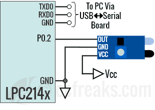
Interfacing Potentiometer using ADC on LPC134x

This example performs Analog to Digital conversion in Software Controlled Mode. Here we use PIO0_11(P0.11) as analog input for measuring the voltage. PIO0_11 corresponds to Channel 0 of ADC i.e. AD0. For testing I had used a 10K potentiometer for ADC Interfacing and connected the middle leg of POT to PIO0_11 of my LPC1343 development board. You can also use a 5K potentiometer for this ADC Example. PIO0_11 is marked as AD0 on LPCXpresso board. Schematic for this example is as shown below:

Schematic for ADC interfacing on LPC134x

Source Code :


/*(C) Umang Gajera - www.ocfreaks.com
LPC1343 ADC Interfacing Example 1 Source Code for MCUXpresso
More Embedded tutorials @ www.ocfreaks.com/cat/embedded/
License : GPL.*/

#include <lpc17xx.h>
#include <stdio.h>
#include "ocf_LPC134x_lib.h" //contains code for UART, Timer & to retarget printf().

#define VREF       3.3 //Reference Voltage at VREFP pin, given VREFN = 0V(GND)
#define ADC_CLK_EN (1<<13) //Enable ADC clock
#define SEL_AD0    (1<<0) //Select Channel AD0
#define CLKDIV     15 // ADC clock-divider (ADC_CLOCK=PCLK/CLKDIV+1), yields 4.5Mhz ADC clock
#define ADC_PWRUP  (~(1<<4)) //setting it to 0 will power it up
#define START_CNV  (1<<24) //001 for starting the conversion immediately
#define ADC_DONE   (1U<<31) //define it as unsigned value or compiler will throw warning
#define ADCR_SETUP_SCM (CLKDIV<<8)

int main(void)
{
	//SystemInit(); //Gets called by Startup code, sets CCLK=100Mhz, PCLK=25Mhz
	initUART(); //Initialize UART for printf()
	initTimer0(); //For delayMS()

	LPC_SYSCON->PDRUNCFG &= ADC_PWRUP; //Power-up ADC Block
	LPC_SYSCON->SYSAHBCLKCTRL |= ADC_CLK_EN; //Enable ADC clock
	LPC_ADC->CR =  ADCR_SETUP_SCM | SEL_AD0; //Setup ADC Block

	/* Now select AD0 function and set ADMODE=0 for PIO0_11(P0.11) */
	LPC_IOCON->R_PIO0_11 = 0x2; //Use this for KEIL and LPCXpresso/MCUXpresso - check tutorial for more
	//LPC_IOCON->JTAG_TDI_PIO0_11 = 0x2; //Older version of CMSIS uses this. Uncomment this for CoIDE.

	unsigned int result = 0;

	printf("OCFreaks.com LPC134x ADC Tutorial Example 1.\nSoftware Controlled ADC Mode on AD0 Channel.\n");
	while(1)
	{
		LPC_ADC->CR |= START_CNV; //Start new Conversion
		while((LPC_ADC->DR0 & ADC_DONE) == 0); //Wait until conversion is finished
		result = (LPC_ADC->DR0>>6) & 0x3FF; //10 bit Mask to extract result
		printf("AD0 = %dmV\n" , (int)( result*VREF ));
		delayMS(500); //Slowing down Updates to 2 Updates per second
	}

	//return 0; //This won't execute
}

Serial Output :

LPC1343 ADC Interfacing Example Screenshot

ocf_lpc134x_lib.c header used in project also contains code for retargeting printf() over UART for LPCXpresso/MCUXpresso. The project for CoIDE contains separate printf.c to retarget printf() using UART.

MCUXpresso Project for Example given above is on GitHub @ LPC134x ADC Interfacing Example 1 [Successfully tested on MCUXpresso v10.0.2], Download Project Workspace Zip

CoIDE Project on GitHub @ LPC134x ADC Interfacing Example 1 [Successfully tested on CooCox CoIDE v1.7.8], Download Project Zip

LPC1343 ADC Interrupt Example

Now, lets cover an example using Hardware controlled mode or Burst mode using ADC Interrupt. In this mode we will have to use ADC interrupt since the ADC block will scan the selected channels and generated interrupt when a conversion gets finished on a particular channel. It scans the channels in round-robin fashion.

In this example too, we will use PIO0_11(P0.11) for measuring the voltage. The connections are same as given in example 1. The ADC ISR ADC_IRQHandler() gets called everytime conversion is finished on selected channel.

Source Code:


/*(C) Umang Gajera - www.ocfreaks.com
LPC1343 ADC Interrupt Example Source Code for MCUXpresso
More Embedded tutorials @ www.ocfreaks.com/cat/embedded/
License : GPL.*/

#include <lpc17xx.h>
#include <stdio.h>
#include "ocf_LPC134x_lib.h" //contains code for UART, Timer & to retarget printf().

#define VREF       3.3 //Reference Voltage at VREFP pin, given VREFN = 0V(GND)
#define ADC_CLK_EN (1<<13) //Enable ADC clock
#define SEL_AD0    (1<<0) //Select Channel AD0
#define CLKDIV     15 // ADC clock-divider (ADC_CLOCK=PCLK/CLKDIV+1), yields 4.5Mhz ADC clock
#define ADC_PWRUP  (~(1<<4)) //setting it to 0 will power it up
#define START_CNV  (1<<24) //001 for starting the conversion immediately
#define ADC_DONE   (1U<<31) //define it as unsigned value or compiler will throw warning
#define ADC_BURST  (1<<16) //Enable burst(hardware) mode
#define ADCR_SETUP_BURST ((CLKDIV<<8) | ADC_BURST)

int AD0Result=0;

int main(void)
{
	//SystemInit(); //Gets called by Startup code, sets CCLK=100Mhz, PCLK=25Mhz
	initUART(); //Initialize UART for printf()
	initTimer0(); //For delayMS()

	LPC_SYSCON->PDRUNCFG &= ADC_PWRUP; //Power-up ADC Block
	LPC_SYSCON->SYSAHBCLKCTRL |= ADC_CLK_EN; //Enable ADC clock
	LPC_ADC->CR =  ADCR_SETUP_BURST | SEL_AD0; //Setup ADC Block

	/* Now select AD0 function and set ADMODE=0 for PIO0_11(P0.11) */
	LPC_IOCON->R_PIO0_11 = 0x2; //Use this for KEIL and LPCXpresso/MCUXpresso - check tutorial for more
	//LPC_IOCON->JTAG_TDI_PIO0_11 = 0x2; //Older version of CMSIS uses this. Uncomment this for CoIDE.

	LPC_ADC->INTEN = SEL_AD0; //Enable AD0 Interrupt, set ADGINTEN to 0
	NVIC_EnableIRQ(ADC_IRQn); //Enable ADC IRQ

	printf("OCFreaks.com LPC134x ADC Interrupt Tutorial Example.\n");
	printf("BURST/Hardware-Controlled ADC Mode on AD0 Channel.\n");
	while(1)
	{
		printf("AD0 = %dmV\n" , (int)( AD0Result*VREF ));
		delayMS(500); //Slowing down Updates to 2 Updates per second
	}
	//return 0; //This won't execute
}

void ADC_IRQHandler(void)
{
	unsigned long ADC_GDR_Read = LPC_ADC->GDR;
	int channel = (ADC_GDR_Read>>24) & 0x7; //Extract Channel Number
	int currentResult = (ADC_GDR_Read>>6) & 0x3FF; //Extract Conversion Result

	if(channel == 0)
	{
		AD0Result = LPC_ADC->DR0; //Dummy read to Clear Done bit
		AD0Result = currentResult;
	}
}

MCUXpresso Project for Example given above is on GitHub @ LPC134x ADC Interrupt Example [Successfully tested on MCUXpresso v10.0.2], Download Project Workspace Zip

CoIDE Project on GitHub @ LPC134x ADC Interrupt Example [Successfully tested on CooCox CoIDE v1.7.8], Download Project Zip

The post LPC1343 ADC Programming Tutorial appeared first on OCFreaks!.


Interfacing LDR with LPC2148

$
0
0

This time we will go through a tutorial on Interfacing LDR with ARM7 LPC2148 microcontroller. Light Dependent Resistor (i.e. LDR for short) is basically used to detect the intensity of light and hence, for example, we can detect if a room is dark or lit. They are also as photoresistors or photoconductive cells. The resistance of LDR is inversely proportional to the intensity of light. Hence under dark conditions the resistance typically rises to around 500K to 5M. Under ambient light the resistance is generally around 2K to 10K. Under very bright light its resistance falls down to around few ohms, for example around 2 to 20 ohms.

For the examples covered in this tutorial, we will use the on-chip ADC module of LPC214x microcontroller to interface LDR. You can check my LPC2148 ADC Programming Tutorial for reference. Since we cannot directly connect an LDR to the ADC’s input, we need to convert the resistance into an equivalent voltage. Once we do this it becomes very easy to interface them. By adding another fixed resistor in series we can form a potential divider network and can connect the common of the resister and LDR to ADC’s input pin. Lets call LDR as R1 and the fixed resistor as R2. The voltage Vout at the common terminal is given as:

LDR Voltage Divider Circuit

Now, to implement this we need a suitable value for R2. The value of R2 in voltage-divider is primarily determined by:

  • LDR’s maximum current
  • LDR’s Response curve [Resistance Vs LUX] (which factors in resistance in dark, bright light and ambient light)

Most of the time using 3.3K or 4.7K or 10K resistor as R2 will do the job. But, always check the manufacturer’s datasheet for max operating current. In case you don’t have access to datasheet, then generally a couple of few milliamps must be safe to operate. For the ones which have used (which have come in ~5mm package), generally 1mA to 5mA have not been an issue. Some LDR’s also allow 50mA to 75mA+ max current. In my case a resistor of 4.7K just works fine and gives a good full scale range. Given LPC2148 uses 3.3V as Vcc, a resistor of 4.7K will limit current to 0.7mA max through LDR under very bright conditions.

Example 1 – Reading the voltage divider output:

In this example we will read the voltage divider output, which changes as the intensity of light changes. The ADC will convert the input voltage to a proportional value between 0 and 1023. We can directly use this value(ADC Result) to detect the light intensity. A value of 0 means Dark condition and a value of 1023 means very bright light is present. With this example you can see the output values change as you change the intensity of light. Working with this example you can decide on a cut-off value or a cut-off range to trigger a function. In this example I have retargeted printf() to redirect its output over UART. Here is the schematic for interfacing LDR with ARM7 LPC2148:

LPC214x LDR Interfacing Example 1 Schematic

Source code:


/*(C) Umang Gajera- www.ocfreaks.com
More Embedded tutorials @ www.ocfreaks.com/cat/embedded/
LPC2148 LDR Interfacing Example 1 Source Code for KEIL ARM.
Also see: http://www.ocfreaks.com/lpc2148-adc-programming-tutorial/
License: GPL.*/

#include <lpc214x.h>
#include <stdio.h> //For retargeted printf()
#include "lib_funcs.h" //OCFreaks LPC214x Tutorial Library Header

#define AD06 ((1<<9)|(1<<8)) //Select AD0.6 function for P0.4
#define SEL_AD06 (1<<6)
#define CLKDIV (15-1) // 4Mhz ADC clock (ADC_CLOCK=PCLK/CLKDIV) where "CLKDIV-1" is actually used , in our case PCLK=60mhz  
#define BURST_MODE_OFF (0<<16) // 1 for on and 0 for off
#define PowerUP (1<<21)
#define START_NOW ((0<<26)|(0<<25)|(1<<24)) //001 for starting the conversion immediately
#define ADC_DONE (1UL<<31)

#define VREF 3.3 //Reference Voltage at VREF pin

int main(void)
{
	initClocks(); //Set PCLK = CCLK = 60Mhz - used by: UART, Timer and ADC
	initUART0(); //Initialize UART0 for retargeted printf()
	initTimer0(); //Init Timer for delay functions
	
	PINSEL0 |= AD06 ; //select AD0.6 for P0.4
	int result = 0;
	unsigned long AD0CR_setup = (CLKDIV<<8) | BURST_MODE_OFF | PowerUP; //Setup ADC block
	
	printf("OCFreaks.com LPC214x LDR Interfacing Tutorial - Example 1.\n");
	
	while(1)
	{
		AD0CR =  AD0CR_setup | SEL_AD06; 
		AD0CR |= START_NOW; //Start new Conversion

		while( (AD0DR6 & ADC_DONE) == 0 );
		
		result = (AD0DR6>>6) & 0x3FF; //get the 10bit ADC result

		printf("AD0.6 = %d\n" , result);
		delayMS(500); //Slowing down Updates to 2 Updates per second
	}
	
	//return 0; //This won't execute normally
}
KEIL ARM uV5/uV4 Project for example given above on GitHub @ LDR Interfacing with LPC2148 Example 1 [Successfully tested on Keil uV5.23], Download Project Zip. You can find the HEX file inside objects folder.

Example 2 – Turn on LED when its dark:

This is a classic example for LDRs. Here we will turn-on an LED when we detect low light or dark conditions. Instead of an LED you can also connect a Relay which can then switch on a Bulb or something like heater during night in cold regions. Make sure you keep the LDR away from the LED or Bulb since we are only interested in detecting sunlight and not artificial light in this case. Schematic for this example is given as follows:

LPC214x LDR Interfacing Example 2 Schematic

Source code:


/*(C) Umang Gajera- www.ocfreaks.com
More Embedded tutorials @ www.ocfreaks.com/cat/embedded/
LPC2148 LDR Interfacing Example 2 Source Code for KEIL ARM.
Also see: http://www.ocfreaks.com/lpc2148-adc-programming-tutorial/
License: GPL.*/

#include <lpc214x.h>
#include "lib_funcs.h" //OCFreaks LPC214x Tutorial Library Header

#define AD06 ((1<<9)|(1<<8)) //Select AD0.6 function for P0.4
#define SEL_AD06 (1<<6)
#define CLKDIV (15-1) // 4Mhz ADC clock (ADC_CLOCK=PCLK/CLKDIV) where "CLKDIV-1" is actually used , in our case PCLK=60mhz  
#define BURST_MODE_OFF (0<<16) // 1 for on and 0 for off
#define PowerUP (1<<21)
#define START_NOW ((0<<26)|(0<<25)|(1<<24)) //001 for starting the conversion immediately
#define ADC_DONE (1UL<<31)
#define VREF 3.3 //Reference Voltage at VREF pin

#define CUT_OFF 200 //Define your cut-off value here

int main(void)
{
	initClocks(); //Set PCLK = CCLK = 60Mhz
	initTimer0(); //Init Timer for delay functions
	
	PINSEL0 |= AD06 ; //select AD0.6 for P0.4
	IO0DIR |= (1<<5); //Select P0.5 as output 
	int result = 0;
	unsigned long AD0CR_setup = (CLKDIV<<8) | BURST_MODE_OFF | PowerUP; //Setup ADC block
	
	while(1)
	{
		AD0CR =  AD0CR_setup | SEL_AD06; 
		AD0CR |= START_NOW; //Start new Conversion

		while( (AD0DR6 & ADC_DONE) == 0 );
		
		result = (AD0DR6>>6) & 0x3FF; //get the 10bit ADC result
		
		if(result < CUT_OFF)
		{
			IO0SET = (1<<5); //LED ON
		}
		else
		{
			IO0CLR = (1<<5); //LED OFF
		}
		
		delayMS(100); //wait some time since LDRs don't react immediately.
	}
	//return 0; //This won't execute normally
}
KEIL ARM uV5/uV4 Project for example given above on GitHub @ LDR Interfacing with LPC2148 Example 2 [Successfully tested on Keil uV5.23], Download Project Zip. You can find the HEX file inside objects folder.

The post Interfacing LDR with LPC2148 appeared first on OCFreaks!.

Interfacing LM35 Sensor with LPC2148

$
0
0

In this tutorial we will see how to interface LM35 Temperature sensor with ARM7 LPC2148 Microcontroller. LM35 is a well known low cost temperature sensor. It is directly calibrated in Degrees Celsius meaning that the output voltage is directly proportional to Degrees Celsius readings. Its measurement range is from -55°C to 150°C having typical accuracy(s) of 0.25°C at room temperature and 0.75°C for full range. LM35 also supports a wide range of supply voltage from 4V to 30V and is available in 4 different packages viz. TO-CAN, TO-92, SOIC and TO-220.

LM35 Pinout for TO-92 Package:

LM35 TO-92 Package

Pin 1 (+Vs) is the positive power supply pin, Pin 2 (VOUT) provides the output voltage linearly proportional to temperature and Pin 3 is for Ground.

LM35 can be configured in two ways:

  • Basic Centigrade Temperature Sensor (2°C to 150°C)
  • Full Range Centigrade Temperature sensor (-55°C to 150°C)

For the sake of simplicity, we will use LM35 in basic configuration. The first thing to note when interfacing LM35 with 3.3v MCUs is that LM35 has a supply voltage range of 4V to 30V. Hence, another supply of say 5V would be required to get proper readings. The second thing to note is that the output voltage has a scale factor of 10mV per Degree Centigrade and this is fixed irrespective of what supply voltage you use between 4V to 30V. Hence, the output voltage can go max up to 1.5V and as low as -55mV when configured as Full Range Centigrade Sensor.

When using the Basic configuration we have an output swing of ~0V(20mV) to 1.5V. So, if we use a VREF of 3.3 Volts we get a resolution of 3.3V/1024 = 0.00322V or 3.22mV since LPC2148 has a 10-bit ADC. Considering that LM35’s typical accuracy at room temperature(25°C) is 0.25°C (worst case accuracy = 0.5°C @ 25°C) and scale factor of 10mV/°C, a resolution of 3.22mV barely fits the bill. To get better resolution we can use a lower voltage reference like 1.8V or 2V. For example, using 1.8V reference we get a resolution of 1.75mV. For the interfacing example given below, we will assume a voltage reference of 3.3V which is commonly used on development boards. If these connections are not present on your development board please make sure VREF pin is connected to 3.3V.

LM35 Transfer Function & Output Conversion to °C

The formula for VOUT is given as:

VOUT(mV) = 10mV/°C * T

Using the above formula, with VERF in Volts and Scale-factor in V/°C, we can compute the temperature(T) from 10-bit ADC Result as:

T =
ADC_RESULT * VREF/1024 * 0.01

°C

Which can be simplified as,

T =
ADC_RESULT * VREF * 100/1024

°C

So, when using VREF = 3.3V we get,

T =
ADC_RESULT * 330/1024

°C

Example for LM35 Interfacing with ARM7 LPC2148

Now lets cover a simple programming example. As obvious, we will use the ADC block of LPC214x for interfacing our temperature sensor using reference voltage as mentioned above. We will use UART0 to send the data to terminal. You can refer my LPC2148 ADC Tutorial and UART Tutorial for more. The example project linked below also contains retargeted printf() for KEIL which redirects its output to UART0.

Interfacing Schematic:

Schematic for Interfacing LM35 Temperature sensor with LPC2148

Since we are interfacing with 5V powered device, I have included an optional ADC input protection using a 1K resistor and a 3.3V Zener Diode – just in case anything goes wrong while making the connections or with the temperature sensor.

Source code:


/*(C) Umang Gajera- www.ocfreaks.com
Interfacing LM35 with LPC2148 - Example Source Code for KEIL ARM.
Also see: http://www.ocfreaks.com/lpc2148-adc-programming-tutorial/
More Embedded tutorials @ www.ocfreaks.com/cat/embedded/
License: GPL.*/

#include <lpc214x.h>
#include <stdio.h> //visit http://www.ocfreaks.com/retarget-redirect-printf-scanf-uart-keil/ 
#include "lib_funcs.h" //OCFreaks LPC214x Tutorials Library Header

#define AD06 ((1<<9)|(1<<8)) //Select AD0.6 function for P0.4
#define SEL_AD06 (1<<6) //Select AD0.6 Channel
#define CLKDIV (15-1) //4Mhz ADC clock (ADC_CLOCK=PCLK/CLKDIV) where "CLKDIV-1" is actually used, in our case PCLK=60mhz  
#define BURST_MODE_OFF (0<<16) //1 for on and 0 for off
#define PowerUP (1<<21)
#define START_NOW ((0<<26)|(0<<25)|(1<<24)) //001 for starting the conversion immediately
#define ADC_DONE (1UL<<31)

#define VREF 3.3 //Reference Voltage at VREF pin

int main(void)
{
	initClocks(); //Set PCLK = CCLK = 60Mhz - used by: UART, Timer and ADC
	initUART0();  //Initialize UART0 for retargeted printf()
	initTimer0(); //Init Timer for delay functions
	
	PINSEL0 |= AD06; //select AD0.6 for P0.4
	unsigned long AD0CR_setup = (CLKDIV<<8) | BURST_MODE_OFF | PowerUP; 
	int result = 0;
	float temp = 0;
	
	printf("OCFreaks.com LPC214x LM35 Interfacing Tutorial\n");
	
	AD0CR = AD0CR_setup | SEL_AD06; //Setup ADC block
	
	AD0CR |= START_NOW; //Start new Conversion
	while( (AD0DR6 & ADC_DONE) == 0 );
	//Ignore the first ADC reading.
	
	while(1)
	{
		AD0CR |= START_NOW; //Start new Conversion
		while( (AD0DR6 & ADC_DONE) == 0 );
		
		result = (AD0DR6>>6) & 0x3FF; //get the 10bit ADC result
		
		temp = ((float)result * VREF * 100)/1024; //As per the Equation given in the tutorial

		printf("Temp = %0.1f Deg. Celsius\n" , temp);
		
		delayMS(1000); //1 Update per second
	}
	
	//return 0; //This won't execute normally
}

Screenshot:

Demo Screenshot for Interfacing LM35 Temperature sensor with LPC2148

KEIL ARM uV5/uV4 Project for example given above is on GitHub @ LM35 Temperature Sensor Interfacing with LPC2148 [Successfully tested on Keil uV5.23], Download Project Zip. You can find the HEX file inside objects folder.

Reference(s):

The post Interfacing LM35 Sensor with LPC2148 appeared first on OCFreaks!.

Interfacing ADXL335 Accelerometer with LPC2148

$
0
0

This time we will go through a tutorial on interfacing ADXL335 Accelerometer with ARM7 LPC2148 microcontroller. ADXL335 is a 3-axis acceleration sensor with analog outputs for each axis. The analog outputs are proportional to acceleration along each of the orthogonal axis. It has a minimum measurement range of ±3g where g is acceleration due to gravity at the earth’s surface (9.8m/s2). Most common applications include tilt, motion and shock sensing. The voltage supply range for ADXL335 is 1.8V to 3.6V. ADXL335 is available in 16-lead LFCSP_LQ package.

Output Voltage:

The output voltage(hence sensitivity) for each of the axis is directly proportional(ratiometric) with the supply voltage used. The Zero g bias output is also proportional to the supply voltage. The Zero g output voltage is typically Vs/2 for any given valid supply voltage.

Sensitivity:

Sensitivity is also termed as scale factor for ADXL335 sensor is given in “milli-volts(or volts) per g” i.e. mV/g(or V/g). For a given Supply Voltage Vs, the sensitivity is typically 0.1xVs V/g or Vsx100 mV/g. Hence for a Vs = 3.3V the sensitivity will be typically 330mV/g or 0.33V/g. We will use V/g as unit for sensitivity in the example shown later on.

Converting ADC result to g:

Lets start with the basic formula to convert a 10-bit ADC result into voltage for a given VREF. The sensor output can be computed as:

ADC_Volts =
ADC_RESULT * VREF/1024

V

Lets, also keep units for all voltages in volts. We get the g from ADC result as follows:

g =
ADC_Volts – Zero_G/Sensitivity

Combining the above two equations, with VREF and Vs in Volts, we get,

g =
((ADC_Result*VREF)/1024) – (Vs/2)/0.1*Vs

Interfacing ADXL335 Accelerometer with ARM7 LPC2148 Example:

For interfacing the Accelerometer we will use the ADC block of LPC2148. Since our sensor has 3 outputs we will use AD0.1, AD0.2, AD0.3 to read the output voltages. After fetching the ADC result we can then convert it to g for each axis. In the example given below, we will use UART0 to send the data to terminal. You can refer my LPC2148 ADC Tutorial and UART Tutorial for more. The example project linked below also contains retargeted printf() for KEIL which redirects its output to UART0.

Schematic:

Schematic for Interfacing ADXL335 Accelerometer sensor with LPC2148

Note: Some modules might have on board voltage regulator (and hence extra pins in interface header) which makes it easier to interface with 5V microcontrollers. Please make sure the power supply connections to the module is proper and also change the value of Vs appropriately in your program to get valid results.

main.c source code:


/*(C) Umang Gajera- www.ocfreaks.com
Interfacing ADXL335 Accelerometer sensor with LPC2148 - Example Source Code for KEIL ARM.
Also see: http://www.ocfreaks.com/lpc2148-adc-programming-tutorial/
More Embedded tutorials @ www.ocfreaks.com/cat/embedded/
License: GPL.*/

#include <lpc214x.h>
#include <stdio.h> //visit http://www.ocfreaks.com/retarget-redirect-printf-scanf-uart-keil/ 
#include "lib_funcs.h" //OCFreaks LPC214x Tutorials Library Header

#define SEL_AD01 (1<<1) //Select AD0.1 Channel
#define SEL_AD02 (1<<2) //Select AD0.2 Channel
#define SEL_AD03 (1<<3) //Select AD0.3 Channel
#define CLKDIV   (15-1) //4Mhz ADC clock (ADC_CLOCK=PCLK/CLKDIV) where "CLKDIV-1" is actually used, in our case PCLK=60mhz  
#define BURST_MODE_OFF (0<<16) //1 for on and 0 for off
#define PowerUP   (1<<21)
#define START_NOW ((0<<26)|(0<<25)|(1<<24)) //001 for starting the conversion immediately
#define ADC_DONE  (1UL<<31)

#define VREF 3.3 //Reference Voltage at VREF pin
#define VS 	 3.3 //Supply Voltage for ADXL335
#define ZERO_G (VS/2) //Zero g bias

int main(void)
{
	initClocks(); //Set PCLK = CCLK = 60Mhz - used by: UART, Timer and ADC
	initUART0();  //Initialize UART0 for retargeted printf()
	initTimer0(); //Init Timer for delay functions
	
	PINSEL1 |= (1<<24) | (1<<26) | (1<<28); //select AD0.1/2/3 for P0.28/29/30.
	int adcX,adcY,adcZ;
	float resultVolts,Xg,Yg,Zg;
	unsigned long ADC0CR_Setup = (CLKDIV<<8) | BURST_MODE_OFF | PowerUP;
	printf("OCFreaks.com LPC214x ADXL335 Sensor Interfacing Tutorial\n");
	
	int skipFirst = 1;
	
	while(1)
	{
		AD0CR = ADC0CR_Setup | SEL_AD01 | START_NOW;//Start new Conversion on AD0.1
		while( (AD0DR1 & ADC_DONE) == 0 );
		adcX = (AD0DR1>>6) & 0x3FF; //get the 10bit ADC result
		
		AD0CR = ADC0CR_Setup | SEL_AD02 | START_NOW; //Start new Conversion on AD0.2
		while( (AD0DR2 & ADC_DONE) == 0 );
		adcY = (AD0DR2>>6) & 0x3FF; //get the 10bit ADC result
		
		AD0CR = ADC0CR_Setup | SEL_AD03 | START_NOW; //Start new Conversion on AD0.3
		while( (AD0DR3 & ADC_DONE) == 0 );
		adcZ = (AD0DR3>>6) & 0x3FF; //get the 10bit ADC result
		
		if(skipFirst) //Ignore first ADC readings.
		{
			skipFirst = 0; 
			continue;
		}
		
		//Computing in 2 steps to keep things simple.
		resultVolts = ((float)adcX * VREF) / 1024; //ADC Result converted to millivolts
		Xg = (resultVolts - ZERO_G) / (VS*0.1);
		
		resultVolts = ((float)adcY * VREF) / 1024; //ADC Result converted to millivolts
		Yg = (resultVolts - ZERO_G) / (VS*0.1);
		
		resultVolts = ((float)adcZ * VREF) / 1024; //ADC Result converted to millivolts
		Zg = (resultVolts - ZERO_G) / (VS*0.1);
		
		printf("X=%0.2fg Y=%0.2fg Z=%0.2fg\n", Xg,Yg,Zg);
		
		delayMS(250); //4 Updates per second
	}
	
	//return 0; //This won't execute normally
}

Screenshot:

Demo Screenshot for Interfacing ADXL335 Accelerometer sensor with LPC2148

Project Download:

KEIL ARM uV5/uV4 Project for example given above is on GitHub @ ADXL335 Accelerometer Interfacing with LPC2148 [Successfully tested on Keil uV5.23], Download Project Zip. You can find the HEX file inside objects folder.

Reference(s):

The post Interfacing ADXL335 Accelerometer with LPC2148 appeared first on OCFreaks!.

MSP430 GPIO Programming Tutorial

$
0
0

In this tutorial we will learn MSP430 GPIO Programming. It is also applicable for MSP430x2xx devices like MSP430G2553, MSP430G2231, etc found on Launchpad Development board. Most of the pins on MSP430 Microcontrollers are grouped into a maximum of 8 Ports viz. P1 to P8. Each port is 8-bits wide and has eight associated I/O pins. These pins are directly mapped to the corresponding port registers and hence I/O pins can be manipulated independently. Only pins in Ports P1 and P2 support interrupts. Additionally, each I/O pin also has configurable pull-up and pull-down resistors. Each port has an associated groups of registers used to manipulate its individual pins. The bit mapping and port grouping is as shown below:

MSP430 Digital I/O Port Pin to Register Mapping

MSP430 GPIO registers

The naming convention(as used in the Manual/Datasheet) for Pins is ‘Px.y’ where ‘x’ is the port number (1 to 8) and ‘y’ is simply the pin number (0 to 7) in port ‘x’. For example : P1.1 refers to Pin number 1 of Port 1 , P2.4 refers to Pin number 4 in Port 2. You will see the same conventions used to mark pins on your MSP430 Launchpad development board.

Current version of MSP40G2 Launchpad Ships with MSP430G2553 and MSP430G2452. Older version(Rev1.4) used to ship with MSP430G2231 and MSP430G2211. However, programming is same for all supported devices unless mentioned.

GPIO Registers in MSP430

The GPIO block has many registers. We will only go through some of the digital I/O registers that are within the scope of this tutorial. I will cover Interrupt related registers(viz. PxIFG, PxIES, PxIE) in a different tutorial.

1. PxDIR: This is the GPIO direction control register. Setting any bit to 0 in this register will configure the corresponding Pin[0 to 7] to be used as an Input while setting it to 1 will configure it as Output.

2. PxIN (Readonly): Used to Read values of the Digital I/O pins configured as Input. 0 = Input is LOW, 1 = Input is HIGH.

3. PxOUT: Used to directly write values to pins when pullup/pulldown resistors are disabled. 0 = Output is LOW, 1 = Output is HIGH. When pullup/pulldown resistors are enabled: 0 = Pin is pulled down, 1 = Pin is pulled up.

4. RxREN:For pins configured as input, PxREN is used to enable pullup/down resistor for a given pin and PxOUT in conjunction with PxREN is used to select either Pullup or pulldown resistor. Setting a bit to 1 will enable pullup/down resistor for the corresponding pin while setting it to 0 will disable the same.

PxDIR PxREN PxOUT I/O Config
0 0 X Input with resistors disabled
0 1 0 Input with Internal Pulldown enabled
0 1 1 Input with Internal Pullup enabled
1 X X Output – PxREN has no effect

5. PxSEL & PxSEL2: Since most of the port pins are multiplexed with upto 4 different functions, we need a mechanism to select these functions. This is achived using PxSEL and PxSEL2 registers. The bit combinations of these registers for a particular pin will select a particular pin function. The bit combination is as given below:

PxSEL2(nth bit) PxSEL(nth bit) Pin Function
0 0 GPIO (Digital I/O) Function
0 1 Primary Peripheral Function
1 0 Reserved. Consult device specific datasheet.
1 1 Secondary Peripheral Function

Also note that PxSEL/PxSEL2 registers do not change the pin directions as required by the module function. Make sure you set the proper pin direction, as required by the alternate function, using PxDIR register.

MSP430 GPIO Programming & Example Code in C/C++

Prerequisite: Before we start programming gpio you need to have basic understanding of Binary and Hexadecimal system and Bitwise operations in C/C++, here are two tutorials which can go through (or if you are already acquainted with these you can skip these and continue below) :

msp430.h is common header for all MSP430 devices. This header identifies your device and accordingly includes the device specific header. Each of the device specific headers also include bit definitions viz. from BIT0 to BITF. Where BITn is equivalent to (1<<n) i.e the nth bit location is a 1 and rest bits are 0s.

Now lets see how we can assign values to registers. We can use Hexadecimal notation & decimal notation for assigning values. If your compiler supports other notations like binary notation use can use that too. Lets say, we want to set PIN 6 of Port 1 as output. It can be done in following ways:


CASE 1. P1DIR = (1<<6); //(binary using left shift - direct assign: other pins set to 0)

CASE 2. P1DIR |= 0x20; //or 0x20; (hexadecimal - OR and assign: other pins not affected)

CASE 3. P1DIR |= (1<<6); //(binary using left shift - OR and assign: other pins not affected)

CASE 4. P1DIR |= BIT6; //Same as above, use Standard BIT definitions
  • In many scenarios, Case 1 must be avoided since we are directly assigning a value to the register. So while we are making P1.6 '1' others are forced to be assigned a '0' which can be avoided by ORing and then assigning Value.
  • Case 2 can be used when bits need to be changed in bulk and
  • Case 3(and 4) can be used when some or single bit needs to be changed.

First thing to note here is that preceding Zeros in Hexadecimal Notation can be ignored because they have no meaning since we are working with unsigned values here (positive only) which are assigned to Registers. For eg. 0x4 and 0x04 mean the same.

Note that bit 7 is MSB on extreme left and bit 0 is the LSB on extreme right which represents Big Endian Format. Hence bit 0 is the 1st bit from right , bit 1 is the 2nd bit from right and so on. BIT and PIN Numbers are Zero(0) indexed.

Basic example code in C/C++

Ex. 1)

Consider that we want to configure Pin 0 of Port 1 i.e P1.0 as Output and want to drive it HIGH. This can be done as:


P1DIR |= BIT0; //same as (1<<0) and 0x1, Configure P0.1 as Output
P1OUT |= BIT0; //Drive Output High for P1.0

Ex. 2)

Making output configured Pin P1.4 LOW individually, without affecting other bits can be does as follows:


P1DIR |= BIT4; //Configure P1.4 as Output
P1OUT &= ~BIT4; //Only P1.4 is made LOW

Ex. 3)

Configuring P1.4 and P1.6 as Output and Setting them HIGH together:


P1DIR |= BIT4 | BIT6; //Config P1.4 and P1.6 as Output
P1OUT |= BIT4 | BIT6; //Drive P1.4 and P1.6 HIGHT

Ex. 4)

Configuring all Pins of Port 1 (P1.0 to P1.7) as Output and Setting them High:


P1DIR = 0xFF; //Config all pins of P1 as Output
P1OUT = 0xFF; //Drive all pins HIGH

Ex. 5)

In this example code, we will configure Pin P1.3 as Input with internal Pullup enabled:


P1DIR &= ~BIT3; //Config P1.3 as input (It will be anyways input after reset)
P1REN = BIT3; //Enable Pullup/down for P1.3
P1OUT = BIT3; //Select Pullup resistor for P1.3

Ex. 6)

We can check the current state of Input pin P1.3, configured above, as:


if(P1IN & BIT3)
{
	//P1.3 is HIGH
}
else
{
	//P1.3 is LOW
}

Ex. 7)

Lets, say we have configured P1.4 as input with pullup resistor enabled and we want to continuously scan P1.4 until a LOW appears at the pin. This can be achieved as follows:


P1DIR &= ~BIT4; //Configure P1.4 as Input
P1REN = BIT4; //Enable Pullup/down for P1.4
P1OUT = BIT4; //Select Pullup resistor for P1.4

if(..) //some condition or parent loop
{
	while( !(P1IN & BIT4) ); //wait until P1.4 is LOW (busy wait)
	/*do something after loop terminates*/
}

Real World MSP430 GPIO Examples/Programs

Note: Examples(Demo Programs) given below assume default clock speeds. I have tested below programs using CCS V6.2.0 on MSP430G2231/MSP430G2211 but it will also work on MSP430G2553/MSP430G2452 and other compatible Microcontrollers.

Blinky Example Code

Here we drive pin 0 of port 1 (P1.0) HIGH then LOW in a loop (Toggle). P1.0 is connected to LED1 on Launchpad Development board. We will use the intrinsic function __delay_cycles(unsigned long cycles). As evident, it generates delay by the amount of clock cycles given as argument. However, this is not the recommended method for generating delays and must be avoided. I have used it in example below just for the sake of brevity. We will see how to generate precise delays using Timer in another tutorial.


#include <msp430.h>

int main(void)
{
	WDTCTL = WDTPW | WDTHOLD; //Stop watchdog timer to Prevent PUC Reset
	P1DIR |= BIT0; //Configure P1.0 as Output
	
	while(1)
	{
		P1OUT ^= BIT0; //Toggle P1.0
		__delay_cycles(400000);
	
		/* The above code is same as:
		P1OUT |= BIT0; //Drive P1.0 HIGH - LED1 ON
		__delay_cycles(400000);

		P1OUT &= ~BIT0; //Drive P1.0 LOW - LED1 OFF
		__delay_cycles(400000);	*/
	}
	//return 0; //normally this won't execute
}

Toggle LED with Button Switch

In this example program we will configure P1.3 as Input and monitor it for a LOW on the pin. P.3 is connected to Push Button Switch (S2) on the Launchpad. We will use LED2 i.e. P1.6 as output. Initially LED2 will be ON. Whenever we press the Button S2 it will toggle its State.


#include <msp430.h>

int main(void)
{
	WDTCTL = WDTPW | WDTHOLD; //Stop watchdog timer to Prevent PUC Reset
	P1DIR &= ~BIT3 ; //explicitly making P1.3 as Input - even though by default its Input
	P1REN = BIT3; //Enable Pullup/down
	P1OUT = BIT3; //Select Pullup

	P1DIR |= BIT6; //Configuring P1.6(LED2) as Output
	P1OUT |= BIT6; //drive output HIGH initially

	while(1)
	{
		if( !(P1IN & BIT3) ) //Evaluates to True for a 'LOW' on P1.3
		{
			P1OUT ^= BIT6; //Toggle the state of P1.6
			while( !(P1IN & BIT3) ); //wait until button is released
		}
	}
	//return 0; //this won't execute normally
}

Turn LED ON when Button is pressed else OFF

Now lets modify the above example so that when the button is pressed, LED2 will glow and when released or not pressed the LED won't glow. When switch is not pressed internal pull-up resistor will force the input to a HIGH state.


#include <msp430.h>

int main(void)
{
	WDTCTL = WDTPW | WDTHOLD; //Stop watchdog timer to Prevent PUC Reset
	P1DIR &= ~BIT3 ; //explicitly making P1.3 as Input - even though by default its Input
	P1REN = BIT3; //Enable Pullup/down
	P1OUT = BIT3; //Select Pullup

	P1DIR |= BIT6; //Configuring P1.6(LED2) as Output
	P1OUT &= ~BIT6; //Turn off LED2 initially
	
	while(1)
	{
		if( !(P1IN & BIT3) )
		{
			P1OUT |= BIT6; //Input LOW - turn led ON
		}
		else
		{
			P1OUT &= ~BIT6; //Input HIGH - turn led OFF
		}
	}
	
	//return 0; //normally this won't execute
}

The post MSP430 GPIO Programming Tutorial appeared first on OCFreaks!.

Interfacing IR Sensor with ARM7 LPC2148

$
0
0

In this tutorial we will see how to interface an IR(Infra-Red) photo-diode with ARM7 LPC2148 microcontroller. A photodiode is a diode but additionally also converts light i.e. incident photons into electrical current. An IR photodiode is a photodiode which is sensitive to IR light. These photodiodes are easily identifiable since they are black. An IR diode pair i.e. an IR Photodiode along with an IR LED can be used to sense obstacle or as proximity sensor. It is also used in line-follower robots.

Working principle

IR LED is used as a source of Infra-Red light (Transmitter). A revered-biased IR photodiode (Sensor,Receiver) is used to detect any IR light reflected from objects in front of the pair. When reflected IR light falls on the IR photodiode it generates a small amount of current corresponding to amount of incident light and in this way it acts as an IR sensor. We can then convert this current into voltage to interface with a micrcontroller using ADC. The analog output can also be converted into 1-bit digital output using a comparator. Commonly available IR modules include a comparator(Op-AMP) or a schmitt-trigger and provide 1-bit digital output (HIGH/LOW) to indicate whether an obstacle is present or not. This makes it easy to interface IR diode pair without using ADC.

IR sensor diode working principle

IR Photodiode/LED pair (Rx/Tx) and Modules:

IR photodiode-led RX-TX pair and Proximity sensor line follower Modules

Converting Photo Diode current to Voltage

We can convert the IR photodiode(IR Sensor) current into proportional voltage by using a Load Resistance RL. The reverse bias photodiode current (IPD) flowing through the Load Resistance creates a voltage drop which we can measure. Note that the photodiode is reverse biased and a bias voltage is given. This configuration is also known as photoconductive mode. The configuration where bias voltage is absent is called Photovoltaic mode.

Convert Infra-Red IR photodiode Current to Voltage with Bias

We can also use an Op-AMP/Comparator to convert analog signal into digital signal using a potentiometer to set a threshold voltage which defines the sensing or triggering distance. In the diagram given below, the voltage drop is fed into non-inverting pin of LM393 Comparator as Vin. The middle leg of a 10K potentiometer is connected to inverting pin of LM393 Comparator as Vref which sets the thresholds. Depending on Vin and Vref, the comparator output is either HIGH i.e. Logic 1 or LOW i.e. Logic 0. The condition when the output is either 1 or 0 is given in the diagram. For the circuit given below a HIGH means an obstacle is detected and a LOW means no obstacle is detected. Instead of LM393 you can use any general purpose Op-AMP like LM358/LM324 as a comparator.

IR Proximity sensor obstacle avoidance using LM393 LM358 LM324 op-amp comparator

Similar kind of circuit is present on IR modules used for proximity sensing, obstacle detection, etc. The potentiometer on these modules is used to set the sensing range/distance. Some IR modules used for line-following robots incorporate a schmitt trigger i.e IC 7414 to convert output to digital(HIGH/LOW). The hysteresis curve of schmitt trigger defines a fixed sensing range/distance in these modules.

IR Interfacing Examples with ARM7 LPC2148

Interfacing IR photodiode using LPC214x ADC

In this example we will convert the reverse bias current of IR photodiode into proportional voltage using a 10K resistor in presence of 3.3V(Vcc) biasing voltage. We will use the inbuilt ADC of LPC2148 to convert the voltage into digital readings. You can check my ADC Tutorial for more. We can set a threshold for the digital values to define sensing range. The ADC readings are inversely proportional to the proximity of an object in front. The code is very similar to LDR Interfacing tutorial. The example project linked below also contains retargeted printf() for KEIL which redirects its output to UART0.

Schematic:
Interfacing IR photodiode with LPC2148

Example 1 Source Code:


/*(C) Umang Gajera- www.ocfreaks.com
LPC2148 IR Sensor Interfacing Example 1 Source Code for KEIL ARM.
More Embedded tutorials @ www.ocfreaks.com/cat/embedded/
Also see: http://www.ocfreaks.com/lpc2148-adc-programming-tutorial/
License: GPL.*/

#include <lpc214x.h>
#include <stdio.h> //visit http://www.ocfreaks.com/retarget-redirect-printf-scanf-uart-keil/ 
#include "lib_funcs.h" //OCFreaks LPC214x Tutorials Library Header

#define AD06 ((1<<9)|(1<<8)) //Select AD0.6 function for P0.4
#define SEL_AD06 (1<<6)
#define CLKDIV (15-1) // 4Mhz ADC clock (ADC_CLOCK=PCLK/CLKDIV) where "CLKDIV-1" is actually used , in our case PCLK=60mhz  
#define BURST_MODE_OFF (0<<16) // 1 for on and 0 for off
#define PowerUP (1<<21)
#define START_NOW ((0<<26)|(0<<25)|(1<<24)) //001 for starting the conversion immediately
#define ADC_DONE (1UL<<31)

#define VREF 3.3 //Reference Voltage at VREF pin

int main(void)
{
	initClocks(); //Set PCLK = CCLK = 60Mhz - used by: UART, Timer and ADC
	initUART0(); //Initialize UART0 for retargeted printf()
	initTimer0(); //Init Timer for delay functions
	
	PINSEL0 |= AD06 ; //select AD0.6 for P0.4
	int result = 0;
	unsigned long AD0CR_setup = (CLKDIV<<8) | BURST_MODE_OFF | PowerUP; //Setup ADC block
	
	printf("OCFreaks.com LPC214x IR Sensor Interfacing Tutorial - Example 1.\n");
	
	while(1)
	{
		AD0CR =  AD0CR_setup | SEL_AD06; 
		AD0CR |= START_NOW; //Start new Conversion

		while( (AD0DR6 & ADC_DONE) == 0 );
		
		result = (AD0DR6>>6) & 0x3FF; //get the 10bit ADC result

		printf("AD0.6 = %d\n" , result); //Print raw ADC values corresponding to IR photo-diode reverse current 
		delayMS(500); //Slowing down Updates to 2 Updates per second
	}
	
	//return 0; //This won't execute normally
}
KEIL ARM uV5/uV4 Project for example given above is on GitHub @ IR Sensor Interfacing Example 1 [Successfully tested on Keil uV5.23], Download Project Zip. You can find the HEX file inside objects folder.

Interfacing IR Proximity-Sensor/Obstacle-avoidance Module with ARM7 LPC2148 using GPIO

In this example will interface the IR module using Pin P0.2. Check the output logic of your IR module and edit the code accordingly. For commonly available IR Proximity Sensor modules, a LOW output means an Obstacle is detected else output is HIGH. For line-follower IR modules based on Schimtt-trigger, a HIGH output means an Obstacle is detected else output is LOW.

Schematic:
Interfacing IR proximity sensor module with LPC2148

Example 2 Source Code:


/*(C) Umang Gajera- www.ocfreaks.com
LPC2148 IR Proximity/Obstacle-avoidance Sensor Interfacing Example 2 Source Code for KEIL ARM.
More Embedded tutorials @ www.ocfreaks.com/cat/embedded/
License: GPL.*/

#include <lpc214x.h>
#include <stdio.h> //visit http://www.ocfreaks.com/retarget-redirect-printf-scanf-uart-keil/ 
#include "lib_funcs.h" //OCFreaks LPC214x Tutorials Library Header
#define PIN0_2 (1<<2)

int main(void)
{
	initClocks(); //Set PCLK = CCLK = 60Mhz - used by: UART, Timer
	initUART0(); //Initialize UART0 for retargeted printf()
	initTimer0(); //Init Timer for delay functions

	printf("OCFreaks.com LPC214x IR Sensor Interfacing Tutorial - Example 2.\n");
	
	while(1)
	{
		//Check the O/P Logic of your IR module. Mine gives LOW when obstacle is detected else HIGH.
		if((IO0PIN & PIN0_2) == 0 ) 
		{
			printf("Obstacle Detected!\n");
		}
		else
		{
			printf("No Obstacle ahead.\n");
		}

		delayMS(500); //Slowing down Updates to 2 Updates per second
	}
	
	//return 0; //This won't execute normally
}
KEIL ARM uV5/uV4 Project for example given above is on GitHub @ IR Module Interfacing Example 2 [Successfully tested on Keil uV5.23], Download Project Zip. You can find the HEX file inside objects folder.

The post Interfacing IR Sensor with ARM7 LPC2148 appeared first on OCFreaks!.

Interfacing HC-SR04 Ultrasonic Distance Sensor with LPC2148

$
0
0

In this tutorial we will see how to interface an Ultrasonic distance sensor (HC-SR04) with ARM7 LPC2148 microcontroller. As the name suggests, the HC-SR04 Ultrasonic Distance/Ranging Sensor uses ultrasound to measure distance from a object ahead of the sensor. Ultrasound is a sound wave with frequency greater than the audible limit i.e. > 20Khz. HCSR-04 uses 40Khz ultrasound to measure distance between itself and any object ahead of it with a sensing range of 2 centimeters to 4 meters.

Pinout: The module has got 4 pins viz. VCC(+5V), TRIG, ECHO, GND.

HC-SR04 Sensor Pinout

Working principle

Ultrasonic Distance/Ranging Sensors are based on similar working principle to what is used in SONAR. It has got two transducers, one for transmitting ultrasound and second one for receiving the echo. Based on the time it takes for echo to arrive we can compute the distance, since we already know the speed of sound in air which is around 343 m/s or 1235 km/h (at 20°C).

HC-SR04 Ultrasonic Distance Sensor Working Principle

Interfacing Steps:

  1. To start distance measurement a short pulse of 10us is applied to Trigger pin.
  2. After this the HC-SR04 Module will send a burst of 8 ultrasonic pulses at 40Khz.
  3. It will then output a HIGH for the amount to time taken for the sound waves to reach back.
  4. The pulse HIGH time is measured and then used to calculate the distance.

HC-SR04 Timing Diagram waveform

Distance calculations:

We know speed of sound in air,

Vs = 343 m/s = 0.0343 cm/us

We also know the time it took to sound waves to emit and echo back, lets call it T. Now, by using basic distance formula we can find the distance as:

Distance Traveled = Speed x Time taken
DT = 343 m/s x T seconds

Now, since we will be measuring ECHO ON-Time in microseconds and also to get distance in centimeters we can change the units as follows:

DT in cm = 0.0343 cm/us x T us

After this we divide the computed value by 2 since the waves have traveled double distance.

D =
DT/2

=

0.0343 x T/2

cm

HC-SR04 Ultrasonic sensor Interfacing with ARM7 LPC2148 Example

Now, lets do a programming exercise. For the interfacing example given below, P0.2 is configured as output and connected to TRIG pin and P0.3 is configured as input and connected to ECHO pin of the Ultrasonic Distance sensor. Timer0 module is used for generating delays with 1 us resolution. It is also used to measure time for ECHO pulse using two simple functions viz. startTimer0() & stopTimer0(). You can check the project source code linked below for implementation details. The distance data is sent to Terminal via UART0. You can refer my LPC2148 UART Tutorial for more. The example source code also contains retargeted printf() for KEIL which redirects its output to UART0.

The HC-SR04 Ultrasonic module operates on 5Volts and hence the output HIGH on ECHO pin is also 5V. We can directly interface this on any of the GPIO pin which has a 5V tolerant pad. But its better to use a voltage divider (using 2KΩ and 1KΩ resistors) to get input from ECHO pin for additional safety. Note that we don’t need to translate 3.3V to 5V for TRIG pin since 3.3V is already a HIGH for TTL compatible input pins.

Schematic:

Interfacing schematic circuit diagram for HC-SR04 with ARM7 LPC2148

Source Code:


/*(C) Umang Gajera- www.ocfreaks.com
Interfacing HC-SR04 Ultrasonic Distance/Ranging sensor with LPC2148 - Example Source Code for KEIL ARM.
More Embedded tutorials @ www.ocfreaks.com/cat/embedded/
License: GPL.*/

#include <lpc214x.h>
#include <stdio.h> //visit http://www.ocfreaks.com/retarget-redirect-printf-scanf-uart-keil/ 
#include "lib_funcs.h" //OCFreaks LPC214x Tutorials Library Header

#define TRIG (1<<2) //P0.2
#define ECHO (1<<3) //P0.3

int main(void)
{
	initClocks(); //Set PCLK = CCLK = 60Mhz - used by: UART, Timer and ADC
	initUART0();  //Initialize UART0 for retargeted printf()
	initTimer0(); //Init Timer for delay functions
	int echoTime=0;
	float distance=0;

	IO0DIR |= TRIG;    //Set P0.2(TRIG) as output
	IO0DIR &= ~(ECHO); //Set P0.3(ECHO) as input (explicitly)
	IO0CLR |= TRIG;    //Set P0.2 LOW initially

	printf("OCFreaks.com LPC214x HC-SR04 Sensor Interfacing Tutorial\n");

	while(1)
	{
		//Output 10us HIGH on TRIG pin
		IO0SET |= TRIG;
		delayUS(10);
		IO0CLR |= TRIG;

		while(!(IO0PIN & ECHO)); //Wait for a HIGH on ECHO pin
		startTimer0(); //Start counting
		while(IO0PIN & ECHO); //Wait for a LOW on ECHO pin
		echoTime = stopTimer0(); //Stop counting and save value(us) in echoTime

		distance = (0.0343 * echoTime)/2; //Find the distance

		printf("Distance = %0.2fcm\n",distance);
		
		delayMS(1000); //wait 1 second for next update
	}
	
	//return 0; //This won't execute normally
}

Screenshot:

HC-SR04 Demo Screenshot

Download Project:

KEIL ARM uV5/uV4 Project for example given above is on GitHub @ HCSR04 Ultrasonic Distance Sensor Interfacing with LPC2148 [Successfully tested on Keil uV5.23], Download Project Zip. You can find the HEX file inside objects folder.

The post Interfacing HC-SR04 Ultrasonic Distance Sensor with LPC2148 appeared first on OCFreaks!.

Interfacing LDR with LPC1768

$
0
0

In this tutorial we will see Interfacing of LDR with ARM Cortex-M3 LPC1768 microcontroller. Light Dependent Resistor is the full form of LDR and they are basically used to detect the intensity of light. They are also known as photoresistors or photoconductive cells. The resistance of an LDR is inversely proportional to the intensity of light directly falling on it. Hence under dark conditions the resistance typically rises to around 500KΩ to 5MΩ. Under ambient light the resistance is generally around 2KΩ to 10KΩ. Under very bright light its resistance goes down to around few ohms – in 2 to 20 Ohms range.

For the examples covered in this tutorial, we will use the inbuilt 12bit-ADC module of LPC1768/LPC1769 microcontroller to interface LDR. You can check my LPC1768 ADC Programming Tutorial for reference. Since we cannot directly connect an LDR to the ADC’s input, we need to convert the resistance into an equivalent voltage. By adding another fixed resistor in series we can form a voltage divider network and can connect the common of the resister and LDR to ADC’s input pin. Lets use LDR as R1 and the fixed resistor as R2. The voltage Vout at the common terminal is given as:

LDR Voltage Divider Circuit

Now, to implement this we need a suitable value for R2. The value of R2 in voltage-divider is primarily determined by:

  • LDR’s maximum current
  • LDR’s Response curve [Resistance Vs LUX] (which factors in resistance in dark, bright light and ambient light)

Most of the time using 3.3KΩ or 4.7KΩ or 10KΩ resistor as R2 will do the job. But, always check the manufacturer’s datasheet for max operating current. In case you don’t have access to datasheet, then generally a couple of few milliamps must be safe to operate. For the ones which I have used (which have come in ~5mm package), generally 1mA to 5mA have not been an issue. Some LDR’s also allow 50mA to 75mA+ max current. In my case a resistor of 4.7KΩ just works fine and gives a good full scale range. Given LPC176x uses 3.3V as Vcc, a resistor of 4.7KΩ will limit current to 0.7mA max through LDR under very bright conditions.

Example 1 – Reading the voltage divider output:

In this example we will read the voltage divider output, which changes as the intensity of light changes. The ADC will convert the input voltage to a proportional value between 0 and 4095. We can directly use this value(ADC conversion Result) to detect the intensity of light. A value near 0 means Dark condition and a value near 4096 means very bright light is present. With this example you can see the output values change as you change the intensity of light. Working with this example you can then select a suitable cut-off value or a cut-off range to trigger a function. In this example I have retargeted printf() to redirect its output over UART. The schematic is as shown below:

LPC1768/LPC1769 LDR Interfacing Example 1 Schematic

Source code:


/*(C) Umang Gajera- www.ocfreaks.com
LPC1768/LPC1769 LDR Interfacing Example 1 Source Code for KEIL ARM.
More Embedded tutorials @ www.ocfreaks.com/cat/embedded/
Also see: http://www.ocfreaks.com/lpc1768-adc-programming-tutorial/
License: GPL.*/

#include <lpc17xx.h>
#include <stdio.h> //For retargeted printf() - http://www.ocfreaks.com/retarget-redirect-printf-scanf-uart-keil/ 
#include "ocf_lpc176x_lib.h" //contains initUART0(), initTimer0() & putc() to retarget printf() 

#define ADC_CLK_EN (1<<12) 
#define SEL_AD0_0  (1<<0) //Select Channel AD0.0 
#define CLKDIV     1 //ADC clock-divider (ADC_CLOCK=PCLK/CLKDIV+1) = 12.5Mhz @ 25Mhz PCLK
#define PWRUP      (1<<21) //setting it to 0 will power it down
#define START_CNV  (1<<24) //001 for starting the conversion immediately
#define ADC_DONE   (1U<<31) //define it as unsigned value or compiler will throw #61-D warning
#define ADCR_SETUP_SCM ((CLKDIV<<8) | PWRUP)
//#define VREF       3.3 //Reference Voltage at VREFP pin, given VREFN = 0V(GND) - not used in this example.

int main(void)
{
	//SystemInit(); //Gets called by Startup code, sets CCLK=100Mhz, PCLK=25Mhz
	initUART0(); //Initialize UART0 for retargeted printf() 
	initTimer0(); //For delayMS()

	LPC_SC->PCONP |= ADC_CLK_EN;
	LPC_PINCON->PINSEL1 |= (1<<14); //select AD0.0 for P0.23
	LPC_ADC->ADCR = ADCR_SETUP_SCM | SEL_AD0_0;
	int result = 0;
	
	printf("OCFreaks.com LPC176x LDR Interfacing - Example 1.\n");
	
	while(1)
	{
		LPC_ADC->ADCR |= START_CNV; //Start new Conversion (Software controlled)

		while((LPC_ADC->ADDR0 & ADC_DONE) == 0); //Wait untill conversion is finished
		
		result = (LPC_ADC->ADDR0>>4) & 0xFFF; //12 bit Mask to extract result
		
		printf("AD0.0 = %d\n",result);
		
		delayMS(500); //Slowing down Updates to 2 Updates per second
	}
	
	//return 0; //This won't execute
}
KEIL ARM uV5/uV4 Project for example given above on GitHub @ LDR Interfacing with LPC1768 Example 1 [Successfully tested on Keil uV5.23], Download Project Zip. You can find the HEX file inside objects folder.

Example 2 – Turn on LED when its dark:

In this interfacing example we will turn-on an LED when we detect low light or dark conditions. Instead of an LED you can also connect a Relay which can then switch on a Bulb or something like heater during night in cold regions. Make sure you keep the LDR away from the LED or Bulb since we are only interested in detecting sunlight and not artificial light in this case. Schematic for this example is given as follows:

LPC1768/LPC1769 LDR Interfacing Example 2 Schematic

Source code:


/*(C) Umang Gajera- www.ocfreaks.com
LPC1768/LPC1769 LDR Interfacing Example 2 Source Code for KEIL ARM.
More Embedded tutorials @ www.ocfreaks.com/cat/embedded/
Also see: http://www.ocfreaks.com/lpc1768-adc-programming-tutorial/
License: GPL.*/

#include <lpc176x.h>
#include "ocf_lpc176x_lib.h"

#define ADC_CLK_EN (1<<12)
#define SEL_AD0_0  (1<<0) //Select Channel AD0.0 
#define CLKDIV     1 //ADC clock-divider (ADC_CLOCK=PCLK/CLKDIV+1) = 12.5Mhz @ 25Mhz PCLK
#define PWRUP      (1<<21) //setting it to 0 will power it down
#define START_CNV  (1<<24) //001 for starting the conversion immediately
#define ADC_DONE   (1U<<31) //define it as unsigned value or compiler will throw #61-D warning
#define ADCR_SETUP_SCM ((CLKDIV<<8) | PWRUP)
//#define VREF       3.3 //Reference Voltage at VREFP pin, given VREFN = 0V(GND) - not used in this example.

#define LDR_CUT_OFF 750 //Define your cut-off value here

int main(void)
{
	//SystemInit(); //Gets called by Startup code, sets CCLK=100Mhz, PCLK=25Mhz
	initTimer0(); //For delayMS()

	LPC_SC->PCONP |= ADC_CLK_EN;
	LPC_PINCON->PINSEL1 |= (1<<14); //select AD0.0 for P0.23
	LPC_ADC->ADCR = ADCR_SETUP_SCM | SEL_AD0_0;
	LPC_GPIO0->FIODIR |= (1<<0); //Set P0.0 as output
	LPC_GPIO0->FIOCLR |= (1<<0); //LED initially OFF
	
	int result = 0;
	
	while(1)
	{
		LPC_ADC->ADCR |= START_CNV; //Start new Conversion (Software controlled)

		while((LPC_ADC->ADDR0 & ADC_DONE) == 0);
		
		result = (LPC_ADC->ADDR0>>4) & 0xFFF; //12 bit Mask to extract result
		
		if(result < LDR_CUT_OFF)
		{
			LPC_GPIO0->FIOSET |= (1<<0); //drive P0.0 HIGH - LED ON
		}
		else
		{
			LPC_GPIO0->FIOCLR |= (1<<0); //drive P0.0 LOW - LED OFF
		}
		
		delayMS(50); //wait some time since LDRs don't react immediately.
	}
	//return 0; //This won't execute normally
}
KEIL ARM uV5/uV4 Project for example given above on GitHub @ LDR Interfacing with LPC1768 Example 2 [Successfully tested on Keil uV5.23], Download Project Zip. You can find the HEX file inside objects folder.

The post Interfacing LDR with LPC1768 appeared first on OCFreaks!.


Interfacing DHT11 & DHT22 Sensor with LPC1768

$
0
0

In this tutorial we learn how to interface DHT11 and DHT22 Humidity and Temperature sensor with ARM Cortex-M3 LPC1768 microcontroller. I had discussed basics of DHT11/DHT22 interfacing in my previous tutorial. Please go through it if you are new to DHTxx Humidity and Temperature sensors.

A quick recap of the communication process:

DHT11 DHT22 Humidity and Temperature Sensor communication process protocol

DHT11/DHT22 Data format:

DHT11 DHT22 Humidity and Temperature Sensor data format

Now, lets have a look at steps we need to implement for Programming DTH11/DHT22. Since only one DATA line(PIN) is used, we will use the same GPIO PIN first as OUTPUT to send START condition and then as INPUT to Receive data.

Steps required for DHT11/DHT22 Interfacing:

  1. Configure PIN to be used to communication as OUTPUT.
  2. Set the PIN O/P to LOW and wait for 18 milli-seconds.
  3. Configure the PIN as INPUT. The pull-up resistor will Pull the bus to HIGH.
  4. Wait until DHT responds and pulls the line to LOW after around 40 micro-seconds or else exit as timeout error.
  5. Next, check for 80us LOW followed by 80us HIGH from DHT. This condition denotes that DHT is ready to send data next.
  6. Now, check for 50us LOW followed by 26us to 28us HIGH denoting data bit ‘0’ or 50us LOW followed 70us HIGH denoting data bit ‘1’. Store the interpreted bit in an array. Repeat this for each of 40 bits.
  7. Extract the data bytes from array to record or display it. Optionally the checksum can be used to verify data integrity.
  8. Wait for at least 1 second before starting again to fetch new data.

Program for Interfacing DHT11/DHT22 with ARM LPC1768/LCP1769:

In this example we will use PIN P0.0 (marked as P9 on mbed board) for communication with DHT11 sensor. For DHT22 you just need to make a small change in code to display the decimal part. I leave that to the reader. If you are using the bare 4 pin sensor than make sure that DATA pin is pulled up using 4.7K or 10K resistor. If you are using PCB mounted sensor which has 3 pins then external pullup resistor is not required since it is already present on the PCB. Timer0 module is used for generating delay and measuring timing of responses given by DHTxx. You can go through LPC1768 timer tutorial for reference.

We will also use UART0 to send data back to PC and display it using software terminal. printf() has been targeted such that its output gets redirected to UART0. Checkout my tutorial on how to retarget printf() in keil and LPC1768 UART tutorial for more. The schematic for connections between DHT11 and LPC214x is as given below:

LPC2148 DTH11 Interfacing Schematic

Before going through to source code, first lets go through some the functions used:

  • startTimer0() – Resets counter and Enables Timer0 block.
  • unsigned int stopTimer0() – Disables counting and returns value in T0TC.
  • checkResponse(…) – Used to check the response from DHTxx. It has 3 parameters viz. unsigned int waitTimeUS, unsigned int margin, bool pinValue. waitTimeUS is simply the expected wait time in micro-seconds. Margin is additional timing error or offset we can account for, since the sensor might have intrinsic timing offets. pinValue is the current expected state of pin which it must hold until the given waitTime.
  • char getDataBit() – This checks the pulses for a ‘0’ or a ‘1’ and returns the value accordingly. It will return 2 in case of an error.
  • printError(const char * str) – Prints error message and halts program execution by entering infinite while loop. You must reset board in this situation or you can extend the code to handle errors on the fly.

DHT11 Humidity & Temperature sensor Interfacing Source Code Snippet


/*(C) Umang Gajera - www.ocfreaks.com
DHT11 Humidity and Temperature Sensor Interfacing with LPC1768/LPC1769 Example Source Code for KEIL ARM
More Embedded tutorials @ www.ocfreaks.com/cat/embedded/
License : GPL.*/
#include <lpc17xx.h>
#include <stdio.h> //For retargeted printf() - http://www.ocfreaks.com/retarget-redirect-printf-scanf-uart-keil/
#include "ocf_lpc176x_lib.h" //contains initUART0(), initTimer0() & putc() to retarget printf()

#define LOW 0
#define HIGH 1
void printError(const char * str);
void checkResponse(unsigned int waitTimeUS, unsigned int margin, unsigned char pinValue);
char getDataBit(void);

#define DATA_PIN (1<<0) //Using P0.0 for data communication

int main(void)
{
	unsigned char dataBits[40] = {0};
	char dataBytes[5] = {0};
	
	initTimer0();
	initUART0();
	
	printf("OCFreaks.com - Interfacing DHT11 with LPC1768 Example.\n");
	
	while(1)
	{
		//STEP 1: Set pin to output HIGH which represents idle state
		LPC_GPIO0->FIODIR |= DATA_PIN;
		
		//STEP 2: Pull down pin for 18ms(min) to denote START
		LPC_GPIO0->FIOCLR |= DATA_PIN;
		delayUS(18000); //wait for 18ms
		
		//STEP 3: Pull HIGH and switch to input mode
		//pull-up will pull it HIGH after switching to input mode.
		LPC_GPIO0->FIODIR &= ~(DATA_PIN);
		
		//STEP 4: Wait between 20 to 40us for sensor to respond
		startTimer0();
		while((LPC_GPIO0->FIOPIN & DATA_PIN) != 0)
		{
			if(LPC_TIM0->TC > 40) break; //Timeout
		}
		unsigned int time = stopTimer0();
		
		if(time < 10 || time > 40) 
		{ 
			printError("Failed to communicate with sensor");
		}
		
		//STEP 5: Check for 80us LOW followed by 80us HIGH
		checkResponse(80,5,LOW);
		checkResponse(80,5,HIGH);
		
		//After this DHTxx sends data. Each bit has a preceding 50us LOW. After which 26-28us means '0' and 70us means '1'
		
		//STEP 6: Fetch data
		char data;
		for(int i=0; i < 40; i++)
		{
			data = getDataBit();
			
			if(data == 0 || data == 1)
			{
				dataBits[i] = data;
			}
			else printError("Data Error");
		}
		
		//STEP 7: Extract data bytes from array
		data = 0;
		for(int i=0; i<5; i++) // i is the BYTE counter
		{
			for(int j=0; j<8; j++) // j gives the current position of a bit in i'th BYTE
			{
				if( dataBits[ 8*i + j ] )
					data |= (1<<(7-j)); //we need to only shift 1's by ([BYTESZIE-1] - bitLocation) = (7-j)
			}
			dataBytes[i] = data;
			data = 0;
		}		
		
		printf("Humidity=%d%%, Temp=%d Deg. C\n",dataBytes[0], dataBytes[2]);
		
		//STEP8: Wait for atleast 1 second before probing again
		delayUS(1000000); 
	}
	//return 0;
}

void printError(const char * str)
{
	/*Print error and enter infinite loop to HALT program*/
	printf("%s\n",str);
	while(1);
}

void checkResponse(unsigned int waitTimeUS, unsigned int margin, unsigned char pinValue)
{
	int time = 0;
	int maxwait = waitTimeUS + margin;
	
	startTimer0();
	if(pinValue)
	{
		while(LPC_GPIO0->FIOPIN & DATA_PIN)
		{
			if(LPC_TIM0->TC > (maxwait)) break; 
		}
	}
	else
	{
		while( !(LPC_GPIO0->FIOPIN & DATA_PIN) )
		{
			if(LPC_TIM0->TC > (maxwait)) break; 
		}
	}
	time = stopTimer0();
	
	if(time < (waitTimeUS-margin) || time > maxwait) 
	{
		//printf("Error for wait=%d,margin=%d,pinVal=%d,time=%d\n",waitTimeUS,margin,pinValue,time);
		printError("checkResponse() Error"); //Out of range, including error margin
	}
}

char getDataBit(void)
{
	int time = 0;
	
	checkResponse(50,5,LOW); //Each data bit starts with 50us low
	
	startTimer0();
	while(LPC_GPIO0->FIOPIN & DATA_PIN)
	{
		if(LPC_TIM0->TC > 75)
		{
			return 2; //Error - Timeout for 50us LOW
		}
	}
	time = stopTimer0();
	
	if((time > (27-10)) && (time < (27+10))) //I am getting 21 for HIGH using my DHT11 sensor, so using higher margin
	{
		return 0;
	}
	else if((time > (70-5)) && (time < (70+5)))
	{
		return 1;
	}
	else 
	{ 
		return 2; //Error - Timeout for data pulse
	}
}

Here is a screenshot of the above example in action:

LPC1768 DTH11 DHT22 Humidity and Temperature sensor Interfacing Example output

KEIL ARM uV5 Project for example given above @ DHT11 Interfacing with LPC1768 Example [Successfully tested on Keil uV5.23], Download Project Zip. You can find the HEX file inside objects folder.

The post Interfacing DHT11 & DHT22 Sensor with LPC1768 appeared first on OCFreaks!.

LPC2148 Timer Capture Mode Tutorial with Frequency Counter Example

$
0
0

Following the request of some of our readers, in this tutorial we will cover how to program capture mode for timer module of ARM7 LPC2148 microcontroller along with a frequency counter example using capture input. In my previous LPC2148 Timer tutorial we saw how to setup and program the timer module.

A quick recap:

ARM LPC214x MCUs have two 32-bit-Timer blocks. Each Timer block can be used as a ‘Timer’ or as a ‘Counter’. A timer has a Timer Counter(TC) and Prescale Register(PR) associated with it. TC stores the current value of the count and PR stores a prescalar value. When Timer is Reset and Enabled, TC is set to 0 and incremented by 1 every ‘PR+1’ clock cycles. When it reaches its maximum value it gets reset to 0 and hence restarts counting. PR is used to set the Timer Resolution. When the timer is used in ‘Counter’ mode, and external signal is used to increment the value of TC.

Capture Channels and Input pins

Each timer block has 4 Capture Channels (CAPn.0 to CAPn.3, n=Timer number) associated with it. Using these Capture channels we can take a snapshot(i.e. capture) of the current value of TC when a signal edge is detected. These channels are mapped to device pins. This mapping of Capture Channel to pins is as given below:

Timer0 Timer1
Channel Pin Channel Pin
CAP0.0 P0.2/P0.22/P0.30 CAP1.0 P0.10
CAP0.1 P0.4 CAP1.1 P0.11
CAP0.2 P0.6/P0.16/P0.28 CAP1.2 P0.17/P0.19
CAP0.3 P0.29 CAP1.3 P0.18/P0.21

Using Capture Inputs in ARM7 LPC214x

When using Capture Inputs we use Timer Block in Normal ‘Timer Mode‘ or ‘Counter Mode‘.

  1. In Timer Mode, the Peripheral clock is used as a clock source to increment the Timer Counter(TC) every ‘PR+1’ clock cycles. Whenever a signal edge(rising/falling/both) event is detected, the timestamp i.e. the current value of TC is loaded into corresponding Capture Register(CRx) and optionally we can also generate an interrupt every time Capture Register is loaded with a new value. This behavior is configured using CCR.
  2. In Counter Mode, external signal is used to increment TC every time an edge(rising/falling/both) is detected. This behavior is configured using CTCR. Corresponding bits for Capture channel must be set to zero in CCR. (See register explanation given below)

ARM7 LPC2148 Timer Capture Block diagram

Here is a simple diagram depicting the capture process. Dashed arrows(for both diagrams) signifiy the events.

Microcontroller Input Capture diagram

Capture Related Registers:

Before we start with programming, first lets see the registers. Since I have already discussed main Timer Registers in my LPC2148 Timer tutorial, we will only have a look at registers relating to capture.

1) CCR – Capture Control Register: Used to select which type of Egde(rising/falling/both) is used to Capture Registers (CR0-CR3) and optionally to generate an interrupt when a capture event occurs.

For CR0:

  • Bit 0: Capture on CAPn.0 rising edge. When set to 1, a transition of 0 to 1 on CAPn.0 will cause CR0 to be loaded with the contents of TC. Disabled when 0.
  • Bit 1: Capture on CAPn.0 falling edge. When set to 1, a transition of 1 to 0 on CAPn.0 will cause CR0 to be loaded with the contents of TC. Disabled when 0.
  • Bit 2: Interrupt on CAPn.0 event. When set to 1, a CR0 load due to a CAPn.0 event will generate an interrupt. Disabled when 0.

Similarly bits 3-5, 6-8, 9-11 are for CR1, CR2 & CR3 respectively.

2) CR0 – CR3 – Capture Registers: Each capture register is associated with a Capture Pin. Depending on the settings in CCR, CRn can be loaded with current value of TC when a specific event occurs.

3) CTCR Count Control Register: Used to select between Timer or Counter Mode.
Bits[1:0] – Used to select Timer mode or which Edges can increment TC in counter mode.

  • [00]: Timer Mode. PC is incremented every Rising edge of PCLK.
  • [01]: Counter Mode. TC is incremented on Rising edges on the CAP input selected by Bits[3:2].
  • [10]: Counter Mode. TC is incremented on Falling edges on the CAP input selected by Bits[3:2].
  • [11]: Counter Mode. TC is incremented on Both edges on the CAP input selected by Bits[3:2].

Bits[3:2] – Count Input Select. Only applicable if above bits are not [00].

  • [00]: Used to select CAPn.0 for TIMERn as Count input.
  • [01]: Used to select CAPn.1 for TIMERn as Count input.
  • [10] & [11]: Reserved.

Frequency Counter using LPC2148 Timer Capture

Methods to Measure frequency of an external signal

We will cover two methods of Measuring Unknown Signal Frequency:

  1. By Gating/Probing – In this method we define a Gating Interval in which we count the number of pulses. What is Gating Time? – Gating Time is amount of time for which we probe the input signal. Once we know the no.of. pulses, we can easily deduce the frequency using Gating time. Here we use the external signal as clock source to increment Timer Counter (TC). The value in TC gives the number of pulses counted per Gating Time. This method relies on selecting a proper Gating Time to get valid and accurate results.
  2. By measuring Period using Interrupts – In this method we use an Interrupt Service Routine to find out the time between 2 consecutive pulses i.e. period of the Input signal at that particular instant. This is done using an ISR, but ISR itself is main limiting factor for the maximum frequency which can be measured. Compared to first one, this method can give accurate results, given frequency is below measurement limit.
The maximum input signal frequency which can be reliably measured using first method is half of TIMERn_PCLK, since it takes two successive edges of TIMERn_PCLK to detect one edge of external signal. Hence, using a PCLK of 60Mhz we can measure upto 30Mhz signal properly. For second method we can only measure up to around 1 Mhz due to ISR execution delay & context switching overhead.

For measuring Square wave Signal Frequency, external hardware is not required unless the Pulse HIGH Voltage level is > 3.3 Volts, in which case a Voltage divider or Buffer is mandatory. To measure other Signal types like Saw-tooth, Sine wave we will require something that can provide Hysteresis which will define the HIGH & LOW Voltage Threshold, thereby converting it into a Square signal, to detect any of the edges of the unknown signal. This can be done using a Schmitt Trigger Buffer (either Inverting or Non-Inverting – doesn’t matter).

For both of examples given below, we will use Timer1 module to measure frequency. Capture Channel CAP1.0 is used as capture input. CAP1.0 is mapped to Pin P0.10 on LPC214x, hence we select CAP1.0 alternate function for P0.10.

To generate a square wave signal, I have used LPC214x’s inbuilt PWM module which is configured with 0.05 us resolution. PWM2 output channel is used which gives output on Pin P0.7. Refer my LPC2148 PWM Tutorial for more on PWM. You can also use any external source like a function generator or IC-555 based generator. The example project linked below also contains retargeted printf() for KEIL which redirects its output to UART0.

Schematic

ARM7 LPC2148 Capture Mode Frequency Counter Measurement Example Schematic

1. Frequency Counter Example using Gating/Probing:

In this example we will, we use external signal as clock source for Timer1. Every positive going edge will increment the Timer1 Counter (T1TC) by 1. To count the number of pulses, we start the timer and wait until Gating time. After that we stop the time and read the value in T1TC which gives the no.of. pulses per gating time. For this example I have chosen a gating time of 1 seconds. Obviously, we can get more accurate results using a higher Gating time. For our purpose 1 second is enough to measure signals upto 30Mhz using PCLK=60Mhz. Given Gate time is in ms, the following equation can be used to find the frequency from counted pulses:

Measured Frequency in Khz =
Counted Pulses/Gate Time in ms

Source Code Snippet


/*(C) Umang Gajera- www.ocfreaks.com
ARM7 LPC2148 Input Capture Tutorial - Example 1 for frequency counter using ARM KEIL
More Embedded tutorials @ www.ocfreaks.com/cat/embedded/
License: GPL.*/

#include <lpc214x.h>
#include <stdio.h> //visit http://www.ocfreaks.com/retarget-redirect-printf-scanf-uart-keil/ 
#include "lib_funcs.h" //OCFreaks LPC214x Tutorials Library Header

void initPWM(void); //To generate Test Square wave
unsigned int pulses = 0;
#define GATE_TIME_MS 1000 //Probing/Gating Time in ms

int main(void)
{
	initClocks(); //Set PCLK = CCLK = 60Mhz - used by: UART, Timer & PWM
	initUART0();  //Initialize UART0 for retargeted printf()
	initTimer0(); //Init Timer for delay functions
	
	//Assuming PCLK = 60Mhz
	PINSEL0 |= (1<<21); //Select CAP1.0 for P0.10
	T1CTCR = 0x1; //Increment TC on rising edges of External Signal for CAP1.0
	T1PR = 0; //0.01667us res, 1 clock cycles @60Mhz = 0.01667 us
	T1TCR = 0x02; //Reset Timer
	T1CCR = (1<<0); //Capture on Rising Edge(0->1)
	T1TCR = 0x01; //Enable timer1

	initPWM(); //To generate square wave
	float FreqKhz = 0;
	printf("OCFreaks.com - Measuring Frequency using LCP2148 Timer Capture Ex 1:\n");
	
	while(1)
	{
		
	  T1TCR = 0x1; //Start Timer2
		delayMS(GATE_TIME_MS); //'Gate' signal for defined Time (1 second)
		T1TCR = 0x0; //Stop Timer2
		
		pulses = T1TC; //Read current value in TC, which contains  no.of. pulses counted in 1s
		T1TCR = 0x2; //Reset Timer2 TC
		
		FreqKhz = (double)pulses/GATE_TIME_MS;
		
		if(FreqKhz >= 1000.0) //Display Freq. In MHz
		{
			printf("Frequency = %0.4f MHz\n", FreqKhz/1000.0);
		}
		else //Display Freq. in KHz
		{
			printf("Frequency = %0.2f KHz\n", FreqKhz);
		}
	}

	//return 0; //This won't execute normally
}

void initPWM(void)
{
	//Refer : http://www.ocfreaks.com/lpc2148-pwm-programming-tutorial/
	/*Assuming that PLL0 has been setup with CCLK = 60Mhz and PCLK also = 60Mhz.*/
	/*This is as per the Setup & Init Sequence given in the tutorial*/

	PINSEL0 |= (1<<15); // Select PWM2 output for Pin0.7
	PWMPCR = 0x0; //Select Single Edge PWM - by default its single Edged so this line can be removed
	PWMPR = 3-1; //3 Clock cycles @60Mhz = 0.05us resoultion
	PWMMR0 = 4; //4x0.05 = 0.2us - period duration i.e. 5MHz frequency
	PWMMR2 = 2; //2x0.05 = 0.1us - pulse duration i.e. width
	PWMMCR = (1<<1); // Reset PWMTC on PWMMR0 match
	PWMLER = (1<<2) | (1<<0); // update MR0 and MR2
	PWMPCR = (1<<10); // enable PWM2 output
	PWMTCR = (1<<1) ; //Reset PWM TC & PR

	//Now, the final moment - enable everything
	PWMTCR = (1<<0) | (1<<3); // enable counters and PWM Mode
	//PWM Generation goes active now!!
}

Download Example 1 Project Files:

KEIL ARM uV5/uV4 Project for above example ARM7 LPC214x Frequency Counter Example 1 [Successfully tested on Keil uV5.23], Download Project Zip. You can find the HEX file inside objects folder.

2. Frequency Counter Example using Period Measurement:

Here, a timer resolution of 0.05 micro-seconds is selected by using Prescaler value of 2 (3-1) and PCLK=CLK=60Mhz. We configure the CCR so that the capture occurs for rising edges and an interrupt is also generated. The Timer1 interrupt handler function is the at core of this example where we are measuring the period of the square wave signal. Refer my ARM7 LPC2148 Interrupt Tutorial for more. Here we use 3 global variables viz.. period, previous & current. We just update period with the difference of current and previous. But since the timer counter (TC) is free running, an overflow is bound to occur. So, we need to take care of this condition by detecting an overflow condition which is simply when current is less than previous. In this situation the time difference is calculated as:

Corrected Diff = (TC_MAX * OVF_CNT) + Current - Previous

where, TC_MAX = Maximum value of TC and OVF_CNT = Number of times overflow occurred. Since TC is 32bit, its max value in our case is 0xFFFFFFFF. Also, since we are not measuring extremely low frequency signals OVF_CNT will be at max 1. Another thing is that, if OVF_CNT is >=2 then we will need a datatype of long long (8 bytes) to store the result since we won't be able to store the result in int which is 4 bytes for KEIL ARM compiler.

Hence, the equation boils down to:

Corrected Diff = 0xFFFFFFFF + Current - Previous

Maximum value for frequency of external signal that can be correctly measured depends on the PCLK, Prescalar (PR) and the Latency of Timer Interrupt Routine execution. Out of the three, the main limiting factor is the interrupt latency. For example code given below, I was able to successfully able to measure square wave signals of upto 1Mhz. This frequency limit is more than enough for real-life applications like tachometer interfacing which I will cover in another tutorial.

Source Code Snippet


/*(C) Umang Gajera- www.ocfreaks.com
ARM7 LPC2148 Input Capture Tutorial - Example 2 for frequency counter using ARM KEIL
More Embedded tutorials @ www.ocfreaks.com/cat/embedded/
License: GPL.*/

#include <lpc214x.h>
#include <stdio.h>   //visit http://www.ocfreaks.com/retarget-redirect-printf-scanf-uart-keil/ 
#include "lib_funcs.h" //OCFreaks LPC214x Tutorials Library Header

int main(void)
{
	initClocks(); //Set PCLK = CCLK = 60Mhz - used by: UART, Timer & PWM
	initUART0();  //Initialize UART0 for retargeted printf()
	initTimer0(); //Init Timer for delay functions
	
	//Assuming PCLK = 60Mhz
	PINSEL0 |= (1<<21); //Select CAP1.0 for P0.10
	T1CTCR = 0x0; //Run in Timer Mode
	T1PR = 3-1; //3 Clock cycles @60Mhz = 0.05us resolution
	T1TCR = 0x02; //Reset Timer
	T1CCR = (1<<0) | (1<<2); //Capture on Rising Edge(0->1) and generate an interrupt
	T1TCR = 0x01; //Enable timer1
	
	VICIntEnable |= (1<<5) ; //Enable TIMER1 IRQ
	VICVectCntl0 = (1<<5) | 5; //5th bit must 1 to enable the slot. Refer: http://www.ocfreaks.com/lpc2148-interrupt-tutorial/
	VICVectAddr0 = (unsigned) timer1ISR;

	initPWM(); //Generate Test square wave
	
	printf("OCFreaks.com - Measuring Frequency using Timer Capture\n");
	double frequencyMhz = 0;
	while(1)
	{
		frequencyMhz = (1.0 / (period*0.05) ) * 1000; //0.05 is Timer resolution in us
		printf("Frequency = %0.2f Khz\n",frequencyMhz);
		delayMS(500); //2 Udpates per second
	}
	
	//return 0; //This won't execute normally
}

__irq void timer1ISR(void)
{
	current = T1CR0;

	if(current < previous) //TC has overflowed
	{
		period = 0xFFFFFFFF + current - previous;
	}
	else
	{
		period = current - previous;
	}
	
	previous = T1CR0;
	
	T1IR = (1<<4); //write back to clear the interrupt flag
	VICVectAddr = 0x0; //Acknowledge that ISR has finished execution
}

void initPWM(void)
{
	//Refer : http://www.ocfreaks.com/lpc2148-pwm-programming-tutorial/
	/*Assuming that PLL0 has been setup with CCLK = 60Mhz and PCLK also = 60Mhz.*/
	/*This is as per the Setup & Init Sequence given in the tutorial*/

	PINSEL0 |= (1<<15); // Select PWM2 output for Pin0.7
	PWMPCR = 0x0; //Select Single Edge PWM - by default its single Edged so this line can be removed
	PWMPR = 3-1; //3 Clock cycles @60Mhz = 0.05us
	PWMMR0 = 20; //20x0.05 = 1us - period duration i.e. 1MHz frequency
	PWMMR2 = 10; //10x0.05 = 0.5us - pulse duration i.e. width
	PWMMCR = (1<<1); // Reset PWMTC on PWMMR0 match
	PWMLER = (1<<2) | (1<<0); // update MR0 and MR2
	PWMPCR = (1<<10); // enable PWM2 output
	PWMTCR = (1<<1) ; //Reset PWM TC & PR

	//Now, the final moment - enable everything
	PWMTCR = (1<<0) | (1<<3); // enable counters and PWM Mode
	//PWM Generation goes active now!!
}

In the Frequency Counter Program given above, you can increase the values for PWMMR0 and PWMMR2 to measure other lower frequencies. Trying measure frequencies >1Mhz will yield in incorrect measurement.

KEIL ARM uV5/uV4 Project for above example ARM7 LPC214x Frequency Counter Example 2 [Successfully tested on Keil uV5.23], Download Project Zip. You can find the HEX file inside objects folder.

The post LPC2148 Timer Capture Mode Tutorial with Frequency Counter Example appeared first on OCFreaks!.

Interfacing LM35 Temperature Sensor with LPC1768

$
0
0

In this tutorial I will discuss the interfacing of LM35 Temperature sensor with ARM Cortex-M3 LPC1768 Microcontroller. LM35 is a well known low cost temperature sensor and is directly calibrated in Degrees Celsius meaning that the output voltage is directly proportional to Degrees Celsius readings. It has a measurement range is between -55°C to 150°C giving typical accuracy(s) of 0.25°C at room temperature and 0.75°C for full range. LM35 Temperature sensor also supports a wide range of supply voltage from 4V to 30V and is available in 4 different packages viz. TO-CAN, TO-92, SOIC and TO-220.

LM35 Pinout for TO-92 Package:

LM35 TO-92 Package

Pin 1 (+Vs) is the positive power supply pin, Pin 2 (VOUT) provides the output voltage linearly proportional to temperature and Pin 3 is for Ground.

LM35 can be configured in two ways giving different ranges:

  • Basic Centigrade Temperature Sensor (2°C to 150°C)
  • Full Range Centigrade Temperature sensor (-55°C to 150°C)

To keep things simple, we will interface LM35 in basic configuration. The first thing to note when interfacing LM35 with 3.3v MCUs, like LPC1768/LPC1769, is that LM35 has a supply voltage range of 4V to 30V. Hence, another supply of say 5V would be required to get proper readings. The second thing to note is that the output voltage has a scale factor of 10mV per Degree Centigrade and this is fixed irrespective of what supply voltage we use apply between 4V to 30V. Hence, the output voltage of LM35 can reach a maximum of 1.5V and a minimum of -55mV when configured as Full Range Centigrade Sensor.

When using the Basic configuration we get an output swing of ~0V(20mV) to 1.5V. So, if we use a VREF of 3.3 Volts we get a resolution of 3.3V/4096 = 0.0008056V or 0.8mV since LPC1768 has a 12-bit ADC. Considering that LM35’s typical accuracy at room temperature(25°C) is 0.25°C (worst case accuracy = 0.5°C @ 25°C) and scale factor of 10mV/°C, a resolution of 0.8mV is more than sufficient.

For the interfacing example given below, we will assume a voltage reference of 3.3V which is commonly used on development boards. If these connections are not present on your development board please make sure VREFP pin is connected to 3.3V reference and VREFN to reference ground (0V).

LM35 Transfer Function & Output Conversion to °C

The formula for VOUT is given as:

VOUT(mV) = 10mV/°C * T

Using the above formula, with VERF in Volts and Scale-factor in V/°C, we can compute the temperature(T) from 12-bit ADC Result as:

T =
ADC_RESULT * VREF/4096 * 0.01

°C

Which can be simplified as,

T =
ADC_RESULT * VREF * 100/4096

°C

So, when using VREF = 3.3V we get,

T =
ADC_RESULT * 330/4096

°C

Example for LM35 Temperature Sensor Interfacing with LPC1768

Now lets go through a simple programming example. As obvious, we will use the ADC block of LPC176x for interfacing our temperature sensor using reference voltage as mentioned above. The result obtained from ADC conversion is converted to temperature(in Deg. Celsius) reading using the equations given above. We will use UART0 to send the data to terminal. You can refer my LPC1768 ADC Tutorial and UART Tutorial for more. The example project linked below also contains retargeted printf() for KEIL which redirects its output to UART0.

LM35 Interfacing Schematic:

Schematic for Interfacing LM35 Temperature sensor with LPC1768 LPC1769

Since we are interfacing with 5V powered device, I have included an optional ADC input protection using a 1K resistor and a 3.3V Zener Diode – just in case anything goes wrong while making the connections or with the temperature sensor.

Source code:


/*(C) Umang Gajera - www.ocfreaks.com
Interfacing LM35 Temperature Sensor with LPC1768/LPC1769 - Example Source Code for KEIL ARM.
Also see: http://www.ocfreaks.com/lpc1768-adc-programming-tutorial/
More Embedded tutorials @ www.ocfreaks.com/cat/embedded/
License: GPL.*/

#include <lpc17xx.h>
#include <stdio.h> //For retargeted printf() - http://www.ocfreaks.com/retarget-redirect-printf-scanf-uart-keil/ 
#include "ocf_lpc176x_lib.h" //contains initUART0(), initTimer0() & putc() to retarget printf() 

#define ADC_CLK_EN (1<<12)
#define SEL_AD0_0  (1<<0) //Select Channel AD0.0 
#define CLKDIV     1 //ADC clock-divider (ADC_CLOCK=PCLK/CLKDIV+1) = 12.5Mhz @ 25Mhz PCLK
#define PWRUP      (1<<21) //setting it to 0 will power it down
#define START_CNV  (1<<24) //001 for starting the conversion immediately
#define ADC_DONE   (1U<<31) //define it as unsigned value or compiler will throw #61-D warning
#define ADCR_SETUP_SCM ((CLKDIV<<8) | PWRUP)
#define VREF       3.3 //Reference Voltage at VREFP pin, given VREFN = 0V(GND) - not used in this example.

int main(void)
{
	//SystemInit(); //Gets called by Startup code, sets CCLK=100Mhz, PCLK=25Mhz
	initUART0(); //Initialize UART0 for retargeted printf() 
	initTimer0(); //For delayMS()

	LPC_SC->PCONP |= ADC_CLK_EN;
	LPC_PINCON->PINSEL1 |= (1<<14); //select AD0.0 for P0.23
	LPC_ADC->ADCR = ADCR_SETUP_SCM | SEL_AD0_0;
	int result = 0;
	float temp = 0;
	
	printf("OCFreaks.com LPC176x LDR Interfacing - Example 1.\n");
	
	while(1)
	{
		LPC_ADC->ADCR |= START_CNV; //Start new Conversion (Software controlled)

		while((LPC_ADC->ADDR0 & ADC_DONE) == 0); //Wait untill conversion is finished
		
		result = (LPC_ADC->ADDR0>>4) & 0xFFF; //12 bit Mask to extract result
		
		temp = ((float)result * VREF * 100)/4096; //As per the Equation given in the tutorial

		printf("Temp = %0.1f Deg. Celsius\n" , temp);
		
		delayMS(500); //Slowing down Updates to 2 Updates per second
	}
	
	//return 0; //This won't execute
}
Download Project
KEIL ARM uV5/uV4 Project for example given above is on GitHub @ LM35 Temperature Sensor Interfacing with LPC1768 [Successfully tested on Keil uV5.23], Download Project Zip. You can find the HEX file inside objects folder.

Screenshot:

Demo Screenshot for Interfacing LM35 Temperature sensor with LPC1768 LPC1769

Reference(s):

The post Interfacing LM35 Temperature Sensor with LPC1768 appeared first on OCFreaks!.

Interfacing HC-SR04 Ultrasonic Distance Sensor with LPC1768

$
0
0

In this tutorial I will discuss, how to interface an Ultrasonic distance sensor (HC-SR04) with ARM Cortex-M3 LPC1768 microcontroller. The HC-SR04 Ultrasonic Distance/Ranging Sensor uses ultrasound to measure distance from a object ahead of the sensor. Ultrasound is a soundwave having frequency greater than the audible limit i.e. > 20Khz. HCSR-04 module uses 40Khz ultrasound to measure distance between itself and any object ahead of it with a sensing range of 2 centimeters to 4 meters.

Pinout: The module has got 4 pins viz. VCC(+5V), TRIG, ECHO, GND.

Working principle

Ultrasonic Distance/Ranging Sensors are based on similar working principle to what is used in SONAR. It has got two transducers, one for transmitting ultrasound and second one for receiving the echo. Based on the time it takes for the echo to arrive we can compute the distance, since we already know the speed of sound in air which is around 343 m/s or 1235 km/h (at 20°C).

HC-SR04 Interfacing Steps:

  1. To start distance measurement a short pulse of 10us is applied to Trigger pin.
  2. After receiving trigger pulse, the HC-SR04 Module sends a burst of 8 ultrasonic pulses at 40Khz.
  3. It will then output a HIGH for the amount to time taken for the sound waves to reach back.
  4. The pulse HIGH time is measured and then used to calculate the distance.

Distance calculations:

We know speed of sound in air,

Vs = 343 m/s = 0.0343 cm/us

We also know the time it took for sound waves to emit and echo back, lets call this time taken T. Now, by using basic distance formula we can find the distance as:

Distance Traveled = Speed x Time taken
DT = 343 m/s x T seconds

Now, since we will be measuring ECHO ON-Time in microseconds and also to get distance in centimeters we can change the units as follows:

DT in cm = 0.0343 cm/us x T us

After this we divide the computed value by 2 since the waves have traveled double distance.

D =
DT/2

=

0.0343 x T/2

cm

HC-SR04 Ultrasonic sensor Interfacing with LPC1768 Example

In the interfacing example given below, P0.0 of LPC176x is configured as output and connected to TRIG pin and P0.1 is configured as input and connected to ECHO pin of the Ultrasonic Distance sensor. Timer0 module is used for generating delays with 1 us resolution. It is also used to measure time for ECHO pulse using two simple functions viz. startTimer0() & stopTimer0(). You can check the project source code linked below for implementation details. The distance data is sent to Terminal via UART0. You can refer my LPC1768 UART Tutorial for more. The example source code also contains retargeted printf() for KEIL which redirects its output to UART0.

The HC-SR04 Ultrasonic module operates on 5 Volts and hence the output HIGH on ECHO pin is also 5V. We can directly interface this on any of the GPIO pin which has a 5V tolerant pad. But its better to use a voltage divider (using 2K and 1K resistors) to get input from ECHO pin for additional safety. Note that we don’t need to translate 3.3V to 5V for TRIG pin since 3.3V is already a HIGH for TTL compatible input pins.

Schematic:

LPC1768 HC-SR04 Interfacing Schematic

Source Code:


/*(C) Umang Gajera - www.ocfreaks.com
Interfacing HC-SR04 Ultrasonic Distance/Ranging sensor with LPC1768/LPC1769 - Example Source Code for KEIL ARM.
More Embedded tutorials @ www.ocfreaks.com/cat/embedded/
License: GPL.*/

#include <lpc17xx.h>
#include <stdio.h> //for printf() - http://www.ocfreaks.com/retarget-redirect-printf-scanf-uart-keil/
#include "ocf_lpc176x_lib.h" //contains initUART0(), initTimer0() & putc() to retarget printf()

#define TRIG (1<<0) //P0.0
#define ECHO (1<<1) //P0.1

int main(void)
{
	//SystemInit(); //Gets called by Startup code, sets CCLK=100Mhz, PCLK=25Mhz
	initUART0(); //Initialize UART0 for retargeted printf() - defined in ocf_lpc176x_lib.c
	initTimer0(); //Init Timer for delay functions - defined in ocf_lpc176x_lib.c
	int echoTime=0;
	float distance=0;

	LPC_GPIO0->FIODIR |= TRIG;    //Set P0.2(TRIG) as output
	LPC_GPIO0->FIODIR &= ~(ECHO); //Set P0.3(ECHO) as input (explicitly)
	LPC_GPIO0->FIOCLR |= TRIG;    //Set P0.2 LOW initially

	printf("OCFreaks.com LPC176x HC-SR04 Sensor Interfacing Tutorial\n");

	while(1)
	{
		//Output 10us HIGH on TRIG pin
		LPC_GPIO0->FIOPIN |= TRIG;
		delayUS(10);
		LPC_GPIO0->FIOCLR |= TRIG;

		while(!(LPC_GPIO0->FIOPIN & ECHO)); //Wait for a HIGH on ECHO pin
		startTimer0(); //Start counting
		while(LPC_GPIO0->FIOPIN & ECHO); //Wait for a LOW on ECHO pin
		echoTime = stopTimer0(); //Stop counting and save value(us) in echoTime

		distance = (0.0343 * echoTime)/2; //Find the distance

		printf("Distance = %0.2fcm\n",distance);
		
		delayMS(1000); //1 update per second
	}
	//return 0; //This won't execute normally
}

Download Project:

KEIL ARM uV5 Project for example given above is on GitHub @ HCSR04 Ultrasonic Distance Sensor Interfacing with LPC1768 [Successfully tested on Keil uV5.23], Download Project Zip. You can find the HEX file inside objects folder.

Screenshot:

LPC176x HC-SR04 example screenshot

The post Interfacing HC-SR04 Ultrasonic Distance Sensor with LPC1768 appeared first on OCFreaks!.

Interfacing IR Sensor with LPC1768

$
0
0

In this tutorial we will discuss how to interface an IR(Infra-Red) photo-diode with ARM Cortex-M3 LPC1768 microcontroller. Its also applicable to LPC1769 and other devices of same family. A photodiode is a diode which additionally converts light i.e. incident photons into electrical current. An IR photodiode is a photodiode which is sensitive to IR light. These photodiodes are easily identifiable since they are black. An IR diode pair i.e. an IR Photodiode along with an IR LED can be used to sense obstacle or as proximity sensor. It is also used in line-follower and similar robots.

Working principle

An IR LED is used as a source of Infra-Red light (i.e. a Transmitter). A revered-biased IR photodiode (Sensor, i.e. a Receiver) is used to detect any IR light reflected from objects in front of the pair. When reflected IR light falls on the IR photodiode it generates a small amount of current corresponding to amount of incident light and in this way it acts as an IR sensor. We can then convert this current into voltage to interface with a micrcontroller using ADC. The analog output can also be converted into 1-bit digital output using a comparator. Commonly available IR modules include a comparator(Op-AMP) or a schmitt-trigger and provide 1-bit digital output (HIGH/LOW) to indicate whether an obstacle is present or not. This makes it easy to interface IR diode pair without using ADC.

IR sensor diode working principle

IR Photodiode/LED pair (Rx/Tx) and Modules:

IR photodiode-led RX-TX pair and Proximity sensor line follower Modules

Converting Photo Diode current to Voltage

The IR photodiode(IR Sensor) current can be converted into proportional voltage by using a Load Resistance RL. The reverse bias photodiode current (IPD) flowing through the Load Resistance creates a voltage drop which we can measure. Note that the photodiode is reverse biased and a bias voltage is given. This configuration is also known as photoconductive mode. The configuration where bias voltage is absent is called Photovoltaic mode.

Convert Infra-Red IR photodiode Current to Voltage with Bias

We can also use an Op-AMP/Comparator to convert analog signal into digital signal using a potentiometer to set a threshold voltage which defines the sensing distance. In the diagram given below, the voltage drop is given non-inverting pin of LM393 Comparator as Vin. The middle leg of a 10K potentiometer is connected to inverting pin of LM393 Comparator as Vref which sets the thresholds. Depending on Vin and Vref, the comparator output is either HIGH i.e. Logic 1 or LOW i.e. Logic 0. The condition when the output is either 1 or 0 is given in the diagram. For the circuit given below a logic HIGH means an obstacle is detected and a logic LOW means no obstacle is detected. Instead of LM393 you can use any general purpose Op-AMP like LM358/LM324 as a comparator.

IR Proximity sensor obstacle avoidance using LM393 LM358 LM324 op-amp comparator

Similar kind of circuit is present on IR modules used for proximity sensing, obstacle detection, etc. The potentiometer on these modules is used to set the sensing range/distance. Some IR modules used for line-following robots incorporate a schmitt trigger i.e IC 7414 to convert output to digital(HIGH/LOW). The hysteresis curve of schmitt trigger defines a fixed sensing range/distance in these modules.

IR Interfacing Examples with LPC1768

Interfacing IR photodiode using LPC176x ADC

In this example we will convert the reverse bias current of IR photodiode into proportional voltage using a 10K resistor in presence of 3.3V(Vcc) biasing voltage. We will use the inbuilt 12-bit ADC of LPC1768 to convert the voltage into digital readings. You can check my ADC Tutorial for more. We can set a threshold for the digital values to define sensing range. The ADC readings are inversely proportional to the proximity of an object in front. The code is very similar to LPC176x LDR Interfacing tutorial. The example project linked below also contains retargeted printf() for KEIL which redirects its output to UART0.

Schematic:
Interfacing IR photodiode with LPC1768

Example 1 Source Code:


/*(C) Umang Gajera - www.ocfreaks.com
LPC1768/LPC1769 IR Sensor Interfacing Example 1 Source Code for KEIL ARM.
More Embedded tutorials @ www.ocfreaks.com/cat/embedded/
Also refer: http://www.ocfreaks.com/lpc1768-adc-programming-tutorial/
License : GPL.*/

#include <lpc17xx.h>
#include <stdio.h> //for printf() - http://www.ocfreaks.com/retarget-redirect-printf-scanf-uart-keil/
#include "ocf_lpc176x_lib.h" //contains initUART0(), initTimer0() & putc() to retarget printf()

#define ADC_CLK_EN (1<<12)
#define SEL_AD0_0  (1<<0) //Select Channel AD0.0 
#define CLKDIV     1 //ADC clock-divider (ADC_CLOCK=PCLK/CLKDIV+1) = 12.5Mhz @ 25Mhz PCLK
#define PWRUP      (1<<21) //setting it to 0 will power it down
#define START_CNV  (1<<24) //001 for starting the conversion immediately
#define ADC_DONE   (1U<<31) //define it as unsigned value or compiler will throw #61-D warning
#define ADCR_SETUP_SCM ((CLKDIV<<8) | PWRUP)
#define VREF       3.3 //Reference Voltage at VREFP pin, given VREFN = 0V(GND)

int main(void)
{
	//SystemInit(); //Gets called by Startup code, sets CCLK=100Mhz, PCLK=25Mhz
	initUART0(); //Initialize UART0 for uart_printf() - defined in ocf_lpc176x_lib.c
	initTimer0(); //For delayMS() - defined in ocf_lpc176x_lib.c

	LPC_SC->PCONP |= ADC_CLK_EN;
	LPC_PINCON->PINSEL1 |= (1<<14); //select AD0.0 for P0.23
	LPC_ADC->ADCR =  ADCR_SETUP_SCM | SEL_AD0_0;
	int result = 0;
	
	printf("OCFreaks.com LPC176x IR Sensor Interfacing Tutorial - Example 1.\n");
	
	while(1)
	{
		LPC_ADC->ADCR |= START_CNV; //Start new Conversion

		while((LPC_ADC->ADDR0 & ADC_DONE) == 0); //Wait untill conversion is finished
		
		result = (LPC_ADC->ADDR0>>4) & 0xFFF; //12 bit Mask to extract result
		
		printf("AD0.0 = %d\n" , result); //Display raw result
		
		delayMS(500); //Slowing down Updates to 2 Updates per second
	}
	
	//return 0; //This won't execute
}

Download Project:

KEIL ARM uV5/uV4 Project for example given above is on GitHub @ IR Sensor Interfacing Example 1, Download Project Zip. You can find the HEX file inside objects folder.

Interfacing IR Proximity-Sensor/Obstacle-avoidance Module with LPC1768 using GPIO

In this example will interface the IR module using Pin P0.2. Check the output logic of your IR module and edit the code accordingly. For commonly available IR Proximity Sensor modules, a LOW output means an Obstacle is detected else output is HIGH. For line-follower IR modules based on Schimtt-trigger, a HIGH output means an Obstacle is detected else output is LOW.

Schematic:
Interfacing IR proximity sensor module with LPC1768

Example 2 Source Code:


/*(C) Umang Gajera - www.ocfreaks.com
LPC176x IR Proximity/Obstacle-avoidance Sensor Interfacing Example 2 Source Code for KEIL ARM.
More Embedded tutorials @ www.ocfreaks.com/cat/embedded/
Also refer: http://www.ocfreaks.com/lpc1768-adc-programming-tutorial/
License : GPL.*/

#include <lpc17xx.h>
#include <stdio.h> //for printf() - http://www.ocfreaks.com/retarget-redirect-printf-scanf-uart-keil/
#include "ocf_lpc176x_lib.h" //contains initUART0(), initTimer0() & putc() to retarget printf()
#define PIN0_1 (1<<1)

int main(void)
{
	//SystemInit(); //Gets called by Startup code, sets CCLK=100Mhz, PCLK=25Mhz
	initUART0(); //Initialize UART0 for uart_printf() - defined in ocf_lpc176x_lib.c
	initTimer0(); //For delayMS() - defined in ocf_lpc176x_lib.c
	
	printf("OCFreaks.com LPC176x ADC Tutorial Example 1.\nSoftware Controlled ADC Mode on AD0.0 Channel.\n");
	
	while(1)
	{
		//Check the O/P Logic of your IR module. Mine gives LOW when obstacle is detected else HIGH.
		if((LPC_GPIO0->FIOPIN & PIN0_1) == 0 ) 
		{
			printf("Obstacle Detected!\n");
		}
		else
		{
			printf("No Obstacle ahead.\n");
		}

		delayMS(500); //Slowing down Updates to 2 Updates per second
	}
	//return 0; //This won't execute
}

Download Project:

KEIL ARM uV5/uV4 Project for example given above is on GitHub @ IR Sensor Interfacing Example 2, Download Project Zip. You can find the HEX file inside objects folder.

The post Interfacing IR Sensor with LPC1768 appeared first on OCFreaks!.

LPC2148 Servo Motor Interfacing Tutorial

$
0
0

Hi again folks! In this tutorial we go through interfacing and control of servo motors with ARM7 LPC2148 microcontroller. In my previous tutorial I had explained PWM in ARM7 LPC2148, now its time use PWM block and control servos. RC servos, as the name suggests, are used in RC airplanes, cars and even robots like hexapods, robotic arms, etc. These servos typically accept a PWM signal having a period of 20ms (i.e. a frequency of 50Hz). The commonly used RC servos have a total rotation swing of around 180 degrees(-90 to +90). 0 degree position is called “neutral” which is at the center of the total rotation swing, and hence also called the center position.

  • A pulse width of 500µs or 0.5ms is the minimum pulse width which positions the servo’s output shaft at -90 degrees.
  • A pulse width of 1500µs or 1.5ms positions the servo at 0 degree.
  • Finally a pulse width of 2500µs or 2.5ms is the maximum pulse width which positions the servo at +90 degrees.

Standard servo control pulse for common RC Servo motors

With this information, lets proceed with generating a PWM signal to control servo motors using LPC2148.

PWM signal for RC servos can be generated using Timer or PWM block of LPC214x. Using the PWM block we can generate up to 6 different PWM signals and hence we can control upto 6 servos independently.

Configuring LPC2148 PWM to generate Servo PWM signal

Defining the PWM resolution

Since the PWM pulses vary from 500µs to 2500µs, a resolution of 1µs is more than sufficient. Hence we will configure the PWM block for 1µs resolution and with a period of 20ms(20000µs). Make sure you go through the “PWM Prescaler (PWMPR) Calculations” explained in my LPC2148 PWM tutorial previously. As mentioned previously in that tutorial, the basic formula for working the value of PR given resolution is:

Resolution in Seconds =
PR+1/PCLK in Hz

Since we need resolution is µs scale, we can scale the equation and rewrite it as follows:

Resolution in µs =
PR+1/PCLK in Mhz

Now, to get the value of PR for 1µs Resolution, given we know and have already set PCLK, can be done as follows:

1 µs Resolution =
PR+1/PCLK in MHz

Hence,

PR = (1 x PCLK in MHz) – 1

Finally, since we will be using CCLK=PCLK=60Mhz, we get PR as follows:

PR = (1 x 60) – 1 = 59

Visit my tutorial on LPC2148 PLL and Clock setup for more on how to setup CCLK and PCLK.

Setting up PWM block for 20ms period with output

Now, assuming both CCLK and PCLK are configured to run at 60Mhz, PWM Block can be configured to control RC Servo as follows:

  1. Select the PWMx function on the respective IO pin.
  2. Set PWMPR = 59 to get a resolution of 1us. PWMTC increments every 59+1 Clock cycles @ 60mhz.
  3. Set PWMMCR = 0x1 (bit0 = 1) to Reset PWMTC on PWMMR0 (and , 0x8= interrupt when PWMMR1 matches PWMTC i.e after PWMMR1 reaches the value assigned to it)
  4. Set PWMMR0 = 20000 which sets the period to 20ms for all PWM outputs.
  5. Set PWMMR1 to default PWM pulse time. We will use 1500µs i.e. neutral position.
  6. Set the corresponding bits in PWMLER to update the values in match registers.
  7. Set the corresponding bits PWMPCR to enable PWMx Output.

Example to configure & initialize PWM with PWM1 Output:


PINSEL0 |=  (1<<1); //set Bits [1:0] = 10 to select PWM1 for P0.0

PWMPR = 59; //PWMTC increments every 59+1 Clock cycles @ 60mhz to yield a resolution of 1us
PWMMCR = 0x1; //Reset PWMTC on PWMMR0 Match which defines the PWM period
PWMMR0 = 20000; //PWM period of 20ms
PWMMR1 = 1500; //Default Pulse time. Brings servo in neutral position
PWMLER = (1<<0) | (1<<1); //Enable Match 1 & Match 2 Latch to update new values
PWMPCR = (1<<9); //Enable PWM1 Output
PWMTCR = (1<<1); //Reset PWM Counter
PWMTCR = (1<<0) | (1<<3); //IMP! - Enable Counter and PWM

Updating new PWM/Pulse values:

Once PWM1 output is enabled we need to only update PWM match register 1 i.e. PWMMR1 (& PWMLER) with new values to control our servo's position. For updating new Match values to any of the Match register, the corresponding bit in the Latch Enable Register (PWMLER) must be set to 1. After New values are updated the Latch Enable Bit in PWMLER is again reset. Hence, for every update we must set the corresponding bit in PWMLER to 1. This update will happen at the beginning of next PWM period. For more please read the register explanation given in LPC2148 PWM tutorial previously.

Example for updating PWMMR1:


while(1) //main control loop
{
 //...
 //..
 PWMMR1 = 900;
 PWMLER |= (1<<1); //Bit[1] corresponds to PWMMR1 Latch
 /*new value will be updated at the beginning of next Period*/
 //..
}

ARM7 LPC2148 Servo Interfacing examples

Example 1: Simple Servo Control using LPC214x

In this example we will repeatedly set the servo position to +45, 0, -45 degrees which roughly corresponds to 1ms, 1.5ms and 2ms pulse widths for most RC servos. Here, we will use a delay of 2 seconds between each position. Schematic and Color coding for various servo plugs is also given in the diagram below. Please confirm the color coding of your servo plug before you proceed with any connections.

ARM7 LPC2148 Servo Interfacing wiring connections and schematic

Note: Always double check the polarity of your connections going to servo plug. Connecting it in reserve might damage your servo permanently. The Author cannot be held responsible for any damage arising due to wrong connections for any of examples given here.

Source Code:


/*(C) Umang Gajera - www.ocfreaks.com
LPC2148 Servo Interfacing Tutorial - Example 1
More Embedded tutorials @ www.ocfreaks.com/cat/embedded/
License: GPL.*/

#include <lpc214x.h>
#include "lib_funcs.h" //OCFreaks LPC214x Tutorials Library Header

int main(void)
{
	initClocks(); //Set PCLK = CCLK = 60Mhz
	initTimer0(); //For delay functions

	PINSEL0 |=  (1<<1); //set Bits [1:0] = 10 to select PWM1 for P0.0

	PWMPR = 59; //PWMTC increments every 59+1 Clock cycles @ 60mhz to yield a resolution of 1us
	PWMMCR = 0x1; //Reset PWMTC on PWMMR0 Match which defines the PWM period
	PWMMR0 = 20000; //PWM period of 20ms
	PWMMR1 = 1500; //Default Pulse time. Brings servo in neutral position
	PWMLER = (1<<0) | (1<<1); //Enable Match 1 & Match 2 Latch to update new values
	PWMPCR = (1<<9); //Enable PWM1 Output
	PWMTCR = (1<<1); //Reset PWM Counter
	PWMTCR = (1<<0) | (1<<3); //IMP! - Enable Counter and PWM

	delayMS(2000); //Initial delay
	
	while(1)
	{
		PWMMR1 = 1000; //1ms Pulse
		PWMLER |= (1<<1); //Set MR1 Latch
		delayMS(2000); //2 Secs Delay
		
		PWMMR1 = 1500; //1.5ms Pulse
		PWMLER |= (1<<1);
		delayMS(2000);
		
		PWMMR1 = 2000; //2ms Pulse
		PWMLER |= (1<<1);
		delayMS(2000);
		
		PWMMR1 = 1500; //1.5ms Pulse
		PWMLER |= (1<<1);
		delayMS(2000);
	}
	
	//return 0; //This won't execute normally
}

Project Download:

KEIL ARM uV5/uV4 Project for example given above is on GitHub @ Servo Interfacing with LPC2148 [Successfully tested on Keil uV5.23], Download Project Zip. You can find the HEX file inside objects folder.

Example 2: Sweep/Interpolate Servo between two positions with LPC214x

In this example we will sweep the servo between +45 & -45 degrees. The servo shaft will rotate at constant speed between the two defined locations. Here, we have to play with two parameters which define how smooth and fast will the servo move. These are: the delay between two steps and the step increment. In our case we will use a step increment of 20µs and an inter-step delay of 1 period i.e. 20ms. The wiring is same as shown for example 1.

Source Code:


/*(C) Umang Gajera - www.ocfreaks.com
LPC2148 Servo Interfacing Tutorial - Example 1
More Embedded tutorials @ www.ocfreaks.com/cat/embedded/
License: GPL.*/

#include <lpc214x.h>
#include "lib_funcs.h" //OCFreaks LPC214x Tutorials Library Header

int main(void)
{
	initClocks(); //Set PCLK = CCLK = 60Mhz
	initTimer0(); //For delay functions

	PINSEL0 |=  (1<<1); //set Bits [1:0] = 10 to select PWM1 for P0.0

	PWMPR = 59; //PWMTC increments every 59+1 Clock cycles @ 60mhz to yield a resolution of 1us
	PWMMCR = 0x1; //Reset PWMTC on PWMMR0 Match which defines the PWM perioed
	PWMMR0 = 20000; //PWM period of 20ms
	PWMMR1 = 1000; //Default(starting) Pulse time for sweep.
	PWMLER = (1<<0) | (1<<1); //Enable Match 1 & Match 2 Latch to update new values
	PWMPCR = (1<<9); //Enable PWM1 Output
	PWMTCR = (1<<1); //Reset PWM Counter
	PWMTCR = (1<<0) | (1<<3); //IMP! - Enable Counter and PWM

	delayMS(1000); //Initial delay
	
	int step = 20; //In us
	int stepDelay = 20; //In ms 
	int pulse=1000;
	while(1)
	{
		while(pulse<2000)
		{
			PWMMR1 = pulse;
			PWMLER |= (1<<1);
			delayMS(stepDelay);
			pulse = pulse + step;
		}
		while(pulse>1000)
		{
			PWMMR1 = pulse;
			PWMLER |= (1<<1);
			delayMS(stepDelay);
			pulse = pulse - step;
		}
	}
	
	//return 0; //This won't execute normally
}

Project Download:

KEIL ARM uV5/uV4 Project for example given above is on GitHub @ Servo Interfacing with LPC2148 [Successfully tested on Keil uV5.23], Download Project Zip. You can find the HEX file inside objects folder.

The post LPC2148 Servo Motor Interfacing Tutorial appeared first on OCFreaks!.

LPC1768 Timer Input Capture & Frequency Counter Tutorial

$
0
0

In this tutorial we will go through the programming of input capture mode for timer module of ARM Cortex-M3 LPC1768 microcontroller along with a frequency counter example using capture input. In my previous LPC1768 Timer tutorial we saw how to setup and program the timer module.

Capture Channels and Input pins

Each timer block in LPC176x has 2 Input Capture Channels (CAPn.0 & CAPn.1, n=Timer number). Using these Capture channels we can take a snapshot(i.e. capture) of the current value of TC when a signal edge is detected. These channels are mapped to device pins. This mapping of Capture Channel to pins is as given below:

Timer0 Timer1 Timer2 Timer3
Ch. Pin Ch. Pin Ch. Pin Ch. Pin
CAP0.0 P1.26 CAP1.0 P0.18 CAP2.0 P0.4 CAP3.0 P0.23
CAP0.1 P1.27 CAP1.1 P0.19 CAP2.1 P0.5 CAP3.1 P0.24

Using Capture Inputs in LPC176x

When using Capture Inputs we use Timer Block in Normal ‘Timer Mode‘ or ‘Counter Mode‘.

  1. In Timer Mode, the Peripheral clock is used as a clock source to increment the Timer Counter(TC) every ‘PR+1’ clock cycles. Whenever a signal edge(rising/falling/both) event is detected, the timestamp i.e. the current value of TC is loaded into corresponding Capture Register(CRx) and optionally we can also generate an interrupt every time Capture Register is loaded with a new value. This behavior is configured using CCR.
  2. In Counter Mode, external signal is used to increment TC every time an edge(rising/falling/both) is detected. This behavior is configured using CTCR. Corresponding bits for Capture channel must be set to zero in CCR. (See register explanation given below)

ARM CORTEX-M3 LPC1768 LPC1769 Timer Capture Block diagram

Here is a simple diagram depicting the capture process. Dashed arrows(for both diagrams) signify the events.

Microcontroller Input Capture diagram

Capture Related Registers:

Since I have already discussed main Timer Registers in my LPC1768 Timer tutorial, we will only have a look at registers relating to capture.

1) CCRx – Capture Control Register: Used to select which type of Egde(rising/falling/both) is used to Capture Registers (CR0-CR1) and optionally to generate an interrupt when a capture event occurs.

For CR0:

  • Bit 0: Capture on CAPn.0 rising edge. When set to 1, a transition of 0 to 1 on CAPn.0 will cause CR0 to be loaded with the contents of TC. Disabled when 0.
  • Bit 1: Capture on CAPn.0 falling edge. When set to 1, a transition of 1 to 0 on CAPn.0 will cause CR0 to be loaded with the contents of TC. Disabled when 0.
  • Bit 2: Interrupt on CAPn.0 event. When set to 1, a CR0 load due to a CAPn.0 event will generate an interrupt. Disabled when 0.

Similarly bits 3-5, are for CR1.

2) CR0 & CR1 – Capture Registers: Each capture register is associated with a Capture Pin. Depending on the settings in CCR, CRn can be loaded with current value of TC when a specific event occurs.

3) CTCR Count Control Register: Used to select between Timer or Counter Mode.
Bits[1:0] – Used to select Timer mode or which Edges can increment TC in counter mode.

  • [00]: Timer Mode. PC is incremented every Rising edge of PCLK.
  • [01]: Counter Mode. TC is incremented on Rising edges on the CAP input selected by Bits[3:2].
  • [10]: Counter Mode. TC is incremented on Falling edges on the CAP input selected by Bits[3:2].
  • [11]: Counter Mode. TC is incremented on Both edges on the CAP input selected by Bits[3:2].

Bits[3:2] – Count Input Select. Only applicable if above bits are not [00].

  • [00]: Used to select CAPn.0 for TIMERn as Count input.
  • [01]: Used to select CAPn.1 for TIMERn as Count input.
  • [10] & [11]: Reserved.

Frequency Counter using LPC1768 Timer Capture

Methods to Measure frequency of an external signal

We will cover two methods of Measuring Unknown Signal Frequency:

  1. By Gating/Probing – In this method we define a Gating Interval in which we count the number of pulses. What is Gating Time? – Gating Time is amount of time for which we probe the input signal. Once we know the no.of. pulses, we can easily deduce the frequency using Gating time. Here we use the external signal as clock source to increment Timer Counter (TC). The value in TC gives the number of pulses counted per Gating Time. This method relies on selecting a proper Gating Time to get valid and accurate results.
  2. By measuring Period using Interrupts – In this method we use an Interrupt Service Routine to find out the time between 2 consecutive pulses i.e. period of the Input signal at that particular instant. This is done using an ISR, but ISR itself is main limiting factor for the maximum frequency which can be measured. Compared to first one, this method can give accurate results, given frequency is below measurement limit.
The maximum input signal frequency which can be reliably measured using first method is half of TIMERn_PCLK, since it takes two successive edges of TIMERn_PCLK to detect one edge of external signal. Hence, using a TIMERn_PCLK of 100Mhz we can measure upto 50Mhz signal properly. For second method we can only measure up to around 0.83 Mhz due to ISR execution delay & context switching overhead.

For measuring Square wave Signal Frequency, external hardware is not required unless the Pulse HIGH Voltage level is > 3.3 Volts, in which case a Voltage divider or Buffer is mandatory. To measure other Signal types like Saw-tooth, Sine wave we will require something that can provide Hysteresis which will define the HIGH & LOW Voltage Threshold, thereby converting it into a Square signal, to detect any of the edges of the unknown signal. This can be done using a Schmitt Trigger Buffer (either Inverting or Non-Inverting – doesn’t matter).

For both of examples given below, we will use Timer2 module to measure frequency. Capture Channel CAP2.0 is used as capture input. CAP2.0 is mapped to Pin P0.4 on LPC1768, hence we select CAP2.0 alternate function for P0.4. On mbed platform P0.4 is labelled as p30 and P2.0 as p26. Schematic is also same for both.

To generate a square wave output, we can use LPC176x’s inbuilt PWM module, configured with 0.02 us resolution. PWM1.1 output channel is used which gives output on Pin P2.0. Refer my LPC1768 PWM Tutorial for more on PWM. You can also use any external source like a function generator or IC-555 based generator. The example projects linked below also contain retargeted printf() for KEIL which redirects its output to UART0.

Schematic

ARM Cortex-M3 LPC1768/LPC1769 Capture Mode Frequency Counter Measurement Example Schematic

1. Frequency Counter Example using Gating/Probing:

In this example we will, we use external signal as clock source for Timer2. Every positive going edge will increment the Timer2 Counter (LPC_TIM2->TC) by 1. To count the number of pulses, we start the timer and wait until Gating time. After that we stop the time and read the value in LPC_TIM2->TC which gives the no.of. pulses per gating time. For this example I have chosen a gating time of 1 seconds. Obviously, we can get more accurate results using a higher Gating time. For our purpose 1 second is enough to measure signals upto 50Mhz using TIMER2_PCLK=100Mhz. Given Gate time is in ms, the following equation can be used to find the frequency from counted pulses:

Measured Frequency in Khz =
Counted Pulses/Gate Time in ms

Source Code Snippet


/*(C) Umang Gajera - www.ocfreaks.com
LPC176x Input Capture Tutorial - Example 1(Using Gating) for frequency counter using ARM KEIL
More Embedded tutorials @ www.ocfreaks.com/cat/embedded/
License: GPL.*/

#include <lpc17xx.h>
#include <stdio.h> //for printf() - http://www.ocfreaks.com/retarget-redirect-printf-scanf-uart-keil/
#include "ocf_lpc176x_lib.h" //contains initUART0(), initTimer0() & putc() to retarget printf()

void initPWM(void);
unsigned int pulses = 0;
#define GATE_TIME_MS 1000 // Probing/Gating Time in ms

int main(void)
{
	//SystemInit(); //Gets called by Startup code, sets CCLK=100Mhz, PCLK=25Mhz
	initUART0(); //Initialize UART0 for uart_printf() - see ocf_lpc176x_lib.c
	initTimer0(); //For delayMS() - see ocf_lpc176x_lib.c
	
	/*Using CCLK = 100Mhz and PCLK_TIMER2 = 100Mhz.*/
	LPC_SC->PCONP |= (1<<22); //Power-Up Timer2 module. It is disabled by default.
	LPC_SC->PCLKSEL1 |= (1<<12); //Set bits[13:12] = [01] to select PCLK_TIMER2 = CCLK i.e. 100Mhz in our case. 
	LPC_PINCON->PINSEL0 |= (1<<9) | (1<<8); //Set Bits[9:8] = [11] to Select CAP2.0 for P0.4
	LPC_TIM2->CTCR = 0x1; //Increment TC on rising edges of External Signal for CAP2.0
	LPC_TIM2->PR = 0; //Using lowest PR gives most accurate results
	LPC_TIM2->CCR = 0x0; //Must be [000] for selected CAP input
	LPC_TIM2->TCR = 0x2; //Reset & Disable Timer2 Initially
	
	initPWM(); //To generate square wave signal	
	float FreqKhz = 0;
	printf("OCFreaks.com - LPC1768x Frequency Counter Example 1:\n");

	while(1)
	{
		LPC_TIM2->TCR = 0x1; //Start Timer2
		delayMS(GATE_TIME_MS); //'Gate' signal for defined Time (1 second)
		LPC_TIM2->TCR = 0x0; //Stop Timer2
		
		pulses = LPC_TIM2->TC; //Read current value in TC, which contains  no.of. pulses counted in 1s
		LPC_TIM2->TCR = 0x2; //Reset Timer2 TC
		
		FreqKhz = (double)pulses/GATE_TIME_MS;
		
		if(FreqKhz >= 1000.0) //Display Freq. In MHz
		{
			printf("Frequency = %0.4f MHz\n", FreqKhz/1000.0);
		}
		else //Display Freq. in KHz
		{
			printf("Frequency = %0.2f KHz\n", FreqKhz);
		}
	}
	
	//return 0; //This won't execute normally
}


void initPWM(void)
{
	//Refer: http://www.ocfreaks.com/lpc1768-pwm-programming-tutorial/
	/*Using CCLK = 100Mhz and PCLK_PWM1 = 100Mhz.*/
	
	//By default PWM1 block is powered-on
	LPC_SC->PCLKSEL0 |= (1<<12); //Set bits[13:12] = [01] to select PCLK_PWM1 = CCLK i.e. 100Mhz in our case. 
	LPC_PINCON->PINSEL4 |= (1<<0); // Select PWM1.1 output for Pin2.0
	LPC_PWM1->PCR = 0x0; //Select Single Edge PWM - by default its single Edged so this line can be removed
	LPC_PWM1->PR = 0; //PR+1 = 0+1 = 1 Clock cycle @100Mhz = 0.01us = 10ns
	LPC_PWM1->MR0 = 4; //4x0.01 = 0.04us - period duration i.e. 25Mhz Test frequency
	LPC_PWM1->MR1 = 2; //2x0.01 = 0.02us - pulse duration (50% duty cycle)
	LPC_PWM1->MCR = (1<<1); // Reset PWMTC on PWMMR0 match
	LPC_PWM1->LER = (1<<1) | (1<<0); // update MR0 and MR2
	LPC_PWM1->PCR = (1<<9); // enable PWM1.1 output
	LPC_PWM1->TCR = (1<<1) ; //Reset PWM TC & PR

	LPC_PWM1->TCR = (1<<0) | (1<<3); // enable counters and PWM Mode
	//PWM Generation goes active now!!
}

Download Example 1 Project Files:

KEIL ARM uV5/uV4 Project for above example LPC176x Frequency Counter Example 1 [Successfully tested on Keil uV5.23], Download Project Zip. You can find the HEX file inside objects folder.

2. Frequency Counter Example using Period Measurement:

Here, a timer resolution of 0.02us (or 20ns) is selected by using Prescaler value of 1 with PCLK=CCLK=100Mhz. We configure CCR so that the capture occurs for rising edges and an interrupt is also generated.

The main logic of this frequency counter example lies in the Timer2 interrupt handler function itself where we are measuring the period of the square wave signal. Here we use 3 global variables viz.. period, previous & current. We just update period with the difference of current and previous. But since the timer counter (TC) is free running, an overflow is bound to occur. So, we need to take care of this condition by detecting an overflow condition which is simply when current is less than previous. In this situation the time difference is calculated as:

Corrected Diff = (TC_MAX * OVF_CNT) + Current - Previous

where, TC_MAX = Maximum value of TC and OVF_CNT = Number of times overflow occurred. Since TC is 32bit, its max value in our case is 0xFFFFFFFF. Also, since we are not measuring extremely low frequency signals OVF_CNT will be at max 1. Another thing is that, if OVF_CNT is >=2 then we will need a datatype of long long (8 bytes) to store the result since we won't be able to store the result in int which is 4 bytes for KEIL ARM compiler.

Hence, the equation boils down to:

Corrected Diff = 0xFFFFFFFF + Current - Previous
Maximum value for frequency of external signal that can be reliably measured depends on the PCLK, Prescalar (PR) and the execution Latency of Timer Interrupt Routine. Out of the three, the main limiting factor is the interrupt execution latency. If the frequency is too fast, an Interrupt Request (IRQ) will be raised even before current IRQ has been served. If this happens the pending interrupt flag will be set and cpu will immediately serve the same ISR without entering main() function. This will happen back to back and the code inside main() won't execute unless signal frequency is reduced. Also, for measurement to be reliable, NO new IRQ must be raised while ISR is under execution.

Hence, inside ISR we will have to add additional code to indicate this condition using a flag. Inevitably this will increase the interrupt latency, but never the less we will be able reject 'over-the-limit' frequencies without stalling the code inside main(). While testing the code given below I was able to measure frequencies around 833Khz or 0.83Mhz without stalling code inside main.

Source Code Snippet


/*(C) Umang Gajera - www.ocfreaks.com
LPC176x Input Capture Tutorial - Example 2 for Frequency counter using ARM KEIL
More Embedded tutorials @ www.ocfreaks.com/cat/embedded/
License: GPL.*/

#include <lpc17xx.h>
#include <stdio.h> //for printf() - http://www.ocfreaks.com/retarget-redirect-printf-scanf-uart-keil/
#include "ocf_lpc176x_lib.h" //contains initUART0(), initTimer0() & putc() to retarget printf()

void initPWM(void);
unsigned int period = 0;
unsigned int previous = 0;
unsigned int current = 0 ;
int limitFlag = 0;
#define TIMER_RES 0.02 //Depends on Timer PCLK and PR. Used to convert measured period to frequency. 

int main(void)
{
	//SystemInit(); //Gets called by Startup code, sets CCLK=100Mhz, PCLK=25Mhz
	initUART0(); //Initialize UART0 for uart_printf() - see ocf_lpc176x_lib.c
	initTimer0(); //For delayMS() - see ocf_lpc176x_lib.c
	
	/*Using CCLK = 100Mhz and PCLK_TIMER2 = 100Mhz.*/
	LPC_SC->PCONP |= (1<<22); //Power-Up Timer2 module. It is disabled by default.
	LPC_SC->PCLKSEL1 |= (1<<12); //Set bits[13:12] = [01] to select PCLK_TIMER2 = CCLK i.e. 100Mhz in our case. 
	LPC_PINCON->PINSEL0 |= (1<<9) | (1<<8); //Set Bits[9:8] = [11] to Select CAP2.0 for P0.4
	LPC_TIM2->CTCR = 0x0;
	LPC_TIM2->PR = 1; //PR+1 = 1+1 = 2 clock cycles @ 100Mhz = 0.02us res
	LPC_TIM2->TCR = 0x02; //Reset Timer
	LPC_TIM2->CCR = (1<<0) | (1<<2); //Capture on Rising Edge(0->1) and generate an interrupt
	LPC_TIM2->TCR = 0x01; //Enable timer1
	
	NVIC_EnableIRQ(TIMER2_IRQn); //Enable TIMER2 IRQ
	initPWM(); //To generate square wave	
	
	printf("OCFreaks.com - Frequency Counter Example 2\n");

	while(1)
	{
		if(limitFlag)
		{
			printf("Input Frequency limit reached!\n");
			NVIC_EnableIRQ(TIMER2_IRQn); //Try to measure signal frequency again
			delayMS(500);
		}
		else
		{
			printf("Frequency = %0.2f Khz\n",((1.0/(period*TIMER_RES)) * 1000)); //Convert to frequency, 0.02 is Timer resolution
			delayMS(500); //2 Udpates per second
		}
	}
	
	//return 0; //This won't execute normally
}

void TIMER2_IRQHandler(void)
{
	LPC_TIM2->IR |= (1<<4); //Clear Interrupt Flag
	current = LPC_TIM2->CR0;
	if(current < previous) //TC has overflowed
	{
		period = 0xFFFFFFFF + current - previous;
	}
	else
	{
		period = current - previous;
	}
	previous = current; //LPC_TIM2->CR0;
	
	if(period < 60)
	{
		NVIC_DisableIRQ(TIMER2_IRQn);
		limitFlag = 1;
	}
	else limitFlag = 0;
}

void initPWM(void)
{
	//Refer: http://www.ocfreaks.com/lpc1768-pwm-programming-tutorial/
	/*Using CCLK = 100Mhz and PCLK_PWM1 = 100Mhz.*/
	
	//By default PWM1 block is powered-on
	LPC_SC->PCLKSEL0 |= (1<<12); //Set bits[13:12] = [01] to select PCLK_PWM1 = CCLK i.e. 100Mhz in our case. 
	LPC_PINCON->PINSEL4 |= (1<<0); // Select PWM1.1 output for Pin2.0
	LPC_PWM1->PCR = 0x0; //Select Single Edge PWM - by default its single Edged so this line can be removed
	LPC_PWM1->PR = 1; //PR+1 = 1+1 = 2 Clock cycles @100Mhz = 0.02us
	LPC_PWM1->MR0 = 80; //80x0.02 = 1.6us - period duration i.e. 625Khz Test frequency
	LPC_PWM1->MR1 = 40; //40x0.02 = 0.8us - pulse duration (50% duty cycle)
	LPC_PWM1->MCR = (1<<1); // Reset PWMTC on PWMMR0 match
	LPC_PWM1->LER = (1<<1) | (1<<0); // update MR0 and MR2
	LPC_PWM1->PCR = (1<<9); // enable PWM1.1 output
	LPC_PWM1->TCR = (1<<1) ; //Reset PWM TC & PR

	LPC_PWM1->TCR = (1<<0) | (1<<3); // enable counters and PWM Mode
	//PWM Generation goes active now!!
}

In the Frequency Counter Program given above, you can increase the values for LPC_PWM1->MR0 and LPC_PWM1->MR1 to measure other lower frequencies. The program will reject frequencies above 833.3 Khz.

Download Example 2 Project Files:

KEIL ARM uV5/uV4 Project for above example LPC176x Frequency Counter Example 2 [Successfully tested on Keil uV5.23], Download Project Zip. You can find the HEX file inside objects folder.

The post LPC1768 Timer Input Capture & Frequency Counter Tutorial appeared first on OCFreaks!.


MSP430 Timer Programming Tutorial

$
0
0

In this tutorial we will go through MSP430 Timer programming for MSP430x2xx devices like MSP430G2553, MSP430G2231 found on Launchpad development board. MSP430G2 devices have two 16-bit timers i.e. Timer_A and Timer_B. Timer_B is slightly different than Timer_A and also has few more features, but it is NOT implemented in both MSP430G2553 and MSP430G2331 micro-controllers. Hence, we will focus on Timer_A for this tutorial.

Introduction

MSP430G2553 has two Timer_As viz. Timer0_A3 and Timer1_A3 which features 3 capture/compare registers while MSP430G2231 has only 1 timer called Timer0_A2 with only 2 capture/compare registers. In addition to Capture, Timer_A also supports PWM outputs and interrupts. They also include a Watchdog Timer (WDT+) which I will discuss in another tutorial.

The naming convention used in datasheet is “Timern_Ax” where n = Timer module number, x = no. of. capture/compare registers supported.

Timer_A supports four different clock sources: ACLK, SMCLK and 2 external sources: TACLK or INCLK. The selected clock source can then be divided by 1,2,4 or 8. The register used for counting is called TAR(16-bit R/W) and can increment or decrement for each rising edge of clock signal. Compared to Timer blocks of other microcontrollers, these MCUs don’t support prescaler.

Timer Modes:

Timer_A supports 4 modes of operation:

  1. Stop Mode: In this mode the Timer is Halted.
  2. Up Mode: Timer repeatedly counts from Zero to value stored in Capture/Compare Register 0 (TACCR0).
  3. Continuous: Timer repeatedly counts from Zero to 0xFFFF, which is maximum value for 16-bit TAR.
  4. Up/Down Mode: Timer repeatedly counts from Zero up to the value in TACCR0 and back down to zero.

Timer Modes in MSP430 microcontrollers

MSP430 Timer Registers

1) TAR – Timer Counter Register: Holds the current count for Timer_A.

2) TACCRx – Timer Capture/Compare Register: In Compare mode, it holds compare value to be compared against TAR. In Capture mode, it holds the current value of TAR when a capture is performed. Maximum value it can store is 0xFFFF since its a 16 bit register.

3) TACTL – Control Register: Used to configure Timer_A. This register is divided as follows:

  • Bit[0] – TAIFG – Timer_A Interrupt Flag. 0 = No interrupt pending, 1 = Interrupt pending.
  • Bit[1] – TAIE – Timer_A Interrupt Enable. 0 = Interrupt Disabled, 1 = Interrupt Enabled.
  • Bit[2] – TACLR – Timer_A clear. Setting this bit resets TAR, clock divider, and the count direction. It is automatically reset and is always read as zero.
  • Bits[5:4] – MCx – Mode Control bits. Used to select between 4 different modes as given:
    [00] = MC_0 – Stop mode: Timer is halted.
    [01] = MC_1 – Up mode: Timer counts up to TACCR0.
    [10] = MC_2 – Continuous mode: Timer counts up to 0xFFFF.
    [11] = MC_3 – Up/down mode: Timer counts up to TACCR0 then down to 0x0000.
  • Bit[7:6] – IDx – Input divider. Selects input clock divider.
    [00] = ID_0 – /1
    [01] = ID_1 – /2
    [10] = ID_2 – /4
    [11] = ID_3 – /8
  • Bits[9:8] TASSELx – Timer_A clock source select.
    [00] = TASSEL_0 – TACLK
    [01] = TASSEL_1 – ACLK
    [10] = TASSEL_2 – SMCLK
    [11] = TASSEL_3 – INCLK (check datasheet)
  • Other Bits – Reserved

3) TACCTLx – Capture/Compare Control Register: Used to configure capture/compare options. I will only cover the parts of this register which are applicable to this tutorial. We will see it in detail in other tutorials(for Capture mode & PWM).

  • Bit[0] – CCIFG – Capture/compare interrupt flag: 0 = interrupt pending, 1 = Interrupt pending.
  • Bit[4] – CCIE – Capture/compare interrupt enable: This bit enables the interrupt request of the corresponding CCIFG flag. 0 = Interrupt disabled = 1 Interrupt enabled.
  • Bit[8] – CAP – Capture mode: Used to select between Compare and Capture mode. We will this bit in its default setting i.e. = 0. 0 = Compare mode, 1 = Capture mode.

4) TAIV – Interrupt Vector Register: Used to identify the flag which requested an interrupt. This is a read only register and only uses 3 bits [3:1] called TAIVx. The values for TAIVx which corresponds to various sources is as given below:

  • 0x00 = No Interrupt Pending.
  • 0x02 = Capture/Compare 1 – TACCR1 CCIFG.
  • 0x04 = Capture/Compare 2 – TACCR2 CCIFG.
  • 0x0A = Timer(TAR) Overflow – TAIFG.
  • Other – Reserved.
Timer Register Naming Convention: Using the register names as given in user manual will default to Timer0_A3 registers. For e.g. TACTL is same as TA0CTL. Note that Timer registers are defined as TAnCTL, TAnCCR0 and so on.. where n = Timer module number(in our case 0 or 1). For Timer1_A3 these names will be TA1CTL, TA1CCR0 and so on. TA0CTL and other Timer0_A3 are just redefined as TACTL, TACCR0 and so on.

Configuring & Setting Up Timer in MSP430

Given, clocks are configured properly, basic setup of Timer_A can be done follows:

  • Set the Compare value in TACCR0 if using Up mode or Up/Down mode. Timer may be stopped by using TACCR0 = 0; and can be started/restarted any time by writing a non-zero compare value in TACCR0 whenever Timer is to be used. Total Counts by timer will be TACCR0 + 1.
  • Set CCIE(Capture/Counter Interrupt Enable) bit in TACCTL0 to enable interrupt for CCR0. We also keep the CAP bit to default value(=0) to enable Compare mode.
  • Select Clock Source, Input Clock divider and Timer mode using TASSELx, IDx, MCx fields respectively.
  • Enable global Interrupts and we are done.
Note that TACCR0 has dedicated interrupt vector. Other TACCRx have common interrupt vector(see TAIVx and section 12.2.6 on page 367 in User Manual).

In examples given below we will use Up mode with input clock source as SMCLK(MCx = MC_1) without an divider(IDx = ID_0 i.e. divide by 1). We will set MCLK and SMCLK to run at 1MHz, both sourcing clock from DCO. This is the default configuration.


TACCR0 = ..; //Compare Value for TAR
TACCTL0 |= CCIE; //Enable interrupt for CCR0.
TACTL = TASSEL_2 + ID_0 + MC_1; //Select SMCLK, SMCLK/1 , Up Mode
_enable_interrupt();
/* More code */

Handy MSP430 Timer Formulae for delay calculations

Formula for amount of time taken to increment TAR count by 1 is given as:

Resolution(Delay per TAR Count) in Seconds =
DIV/Input Clock in Hz

where DIV = Input Clock divider either 1,2,4 or 8.

E.g.: When using divider of /2 and Input clock of 4MHz we get timer resolution as,

Resolution =
2/4 x 106Hz

Seconds = 0.5 x 10⁻⁶ Seconds = 0.5 µS

The time required for TAR to count from 0 and reach TACCR0 (i.e. overflow or TAR period) is given as:

Timer Period in Seconds =
DIV x (TACCR0 + 1)/Input Clock in Hz

We subtract 1 from TACCR0 since TAR counts “TACCR0+1” times to overflow. This is because count starts from 0.

E.g.: When using divider of /2, Input clock of 4MHz and TACCR0 = 1000-1 = 999, we get Timer Period as,

Timer Period =
2 x (999 + 1)/4 x 106Hz

= 0.5 x 1000 x 10-6 S = 500 µS

MSP430 Timer Examples

Now, lets cover 2 Timer examples. Both examples are valid for MSP430G2553 , MSP430G2231 and similar MCUs.

Example 1: A simple Delay function using Interrupt

Of-course, we have the option of using inbuilt function __delay_cycles(..), but wheres the fun if we don’t implement a similar function using Timer? Anyways, in this example we will define a function called delayMS(int msec) which generates delay as per given input in mill-seconds. This function is used in conjunction with Timer_A Interrupt for CCR0. The time is counting, ISR continuously increments an Overflow counter when TAR reaches value in TACCR0. We set the value in TACCR0 such that counting from 0 to TACCR0 takes exactly 1ms, and hence we get a resolution of 1ms for our delay function. This function will give more accurate delay as MCLK increases, since it contains a few statements which eat up proportionate amount CPU cycles. Now, since we are using Timer Clock = 1MHz (SMCLK=1MHz), 1000 ticks will equal to 1ms. Hence, we use TACCR0 = 1000 inside delay function. In general for Y MHz timer clock, Y x 1000 ticks are required for 1ms delay. Before exiting the function we use TACCR0 = 0 to stop the Timer.


#include <msp430.h>

void initTimer_A(void);
void delayMS(int msecs);

unsigned int OFCount;

int main(void)
{
	WDTCTL = WDTPW + WDTHOLD; //Stop watchdog timer
	P1DIR |= BIT0; //Configure P1.0 as Output

	//Set MCLK = SMCLK = 1MHz
	BCSCTL1 = CALBC1_1MHZ;
	DCOCTL = CALDCO_1MHZ;

	initTimer_A();
	_enable_interrupt();

	while(1)
	{
		P1OUT |= BIT0; //Drive P1.0 HIGH - LED1 ON
		delayMS(500); //Wait 0.5 Secs

		P1OUT &= ~BIT0; //Drive P1.0 LOW - LED1 OFF
		delayMS(500); //Wait 0.5 Secs
	}
}

void initTimer_A(void)
{
	//Timer0_A3 Configuration
	TACCR0 = 0; //Initially, Stop the Timer
	TACCTL0 |= CCIE; //Enable interrupt for CCR0.
	TACTL = TASSEL_2 + ID_0 + MC_1; //Select SMCLK, SMCLK/1, Up Mode
}

void delayMS(int msecs)
{
	OFCount = 0; //Reset Over-Flow counter
	TACCR0 = 1000-1; //Start Timer, Compare value for Up Mode to get 1ms delay per loop
	//Total count = TACCR0 + 1. Hence we need to subtract 1.

	while(i<=msecs);

	TACCR0 = 0; //Stop Timer
}

//Timer ISR
#pragma vector = TIMER0_A0_VECTOR
__interrupt void Timer_A_CCR0_ISR(void)
{
	OFCount++; //Increment Over-Flow Counter
}

Example 2: Blinky using MSP430 Timer Interrupt

In this example, instead of using a dedicated delay function we place the blinky code inside the Timer_A Interrupt itself. The Timer initialization code is same as before. The Timer is never stopped and it repeatedly restarts counting when TAR reaches TACCR0 to generate 1ms delay. Similar to previous example, an overflow counter is maintained by ISR itself. We just need to define how much delay(in ms) we require. This is done by defining a MACRO BLINKY_DELAY_MS. Also, note that we won't be using Low Power Mode (LMP0). If you want to use LMP0 than make sure TACCR0 has a suitable maximum value along with higher clock divider, so CPU stays disabled most of the time. In our case we can use TACCR0 = 50000; and use overflow count limit of 10 for 500ms delay. In this way the ISR is called every 50ms when clock divider is 1, and every 200ms when clock divider is 4.


#include <msp430.h>
#define BLINKY_DELAY_MS 500 //Change this as per your needs

void initTimer_A(void);
void delayMS(int msecs);

unsigned int OFCount;

int main(void)
{
	WDTCTL = WDTPW + WDTHOLD; //Stop watchdog timer
	P1DIR |= BIT0; //Configure P1.0 as Output

	//Set MCLK = SMCLK = 1MHz
	BCSCTL1 = CALBC1_1MHZ;
	DCOCTL = CALDCO_1MHZ;

	initTimer_A();
	_enable_interrupt();

	OFCount  = 0;
	TACCR0 = 1000-1; //Start Timer, Compare value for Up Mode to get 1ms delay per loop
	/*Total count = TACCR0 + 1. Hence we need to subtract 1.
	1000 ticks @ 1MHz will yield a delay of 1ms.*/

	while(1);
}

void initTimer_A(void)
{
	//Timer Configuration
	TACCR0 = 0; //Initially, Stop the Timer
	TACCTL0 |= CCIE; //Enable interrupt for CCR0.
	TACTL = TASSEL_2 + ID_0 + MC_1; //Select SMCLK, SMCLK/1 , Up Mode
}

//Timer ISR
#pragma vector = TIMER0_A0_VECTOR
__interrupt void Timer_A_CCR0_ISR(void)
{
	OFCount++;
	if(OFCount >= BLINKY_DELAY_MS)
	{
		P1OUT ^= BIT0;
		OFCount = 0;
	}
}

The post MSP430 Timer Programming Tutorial appeared first on OCFreaks!.

Create new STM32 project in Keil uVision 5 tutorial

$
0
0

In this tutorial we see how to create project in KEIL MDK uVision 5 for STM32 ARM Cortex-M based MCUs. Its for beginners who want to get started in programming STM32 with Keil. This tutorial also applies for all supported devices across the STM32 Family viz. STM32F0/F1/F2/F4/F7/etc/. Keil uV 5 is much different than older Keil uV4. uVision 5 has integrated pack installer which is used to install specific MCU family packs and other libraries. To create project for STM32 MCU, you will first need to install MDK5 software packs for your microcontroller family. Either you can download it separately or do it from within the IDE.I recommend adding software packs using IDE.

Basically three(or more?) types of STM32 Keil projects can be created:

  1. One that uses CMSIS(core) only.
  2. One that is based on Standard Peripheral Library.
  3. Finally, one that is based on HAL (Hardware abstraction Layer) Library.

For the sake of this tutorial we will see how to create CMSIS and SPL based STM32F103C8 Keil uv5 project, as an example, but will work exactly the same for STM32F0, STM32F4, and other families. I will cover HAL based projects in another tutorial.

1) Installing prerequisite STM32 Keil software pack

If already installed, you can SKIP this.

Step A. Download latest Keil MDK uVision5 from Keil’s website.

Step B. Install Keil uVision 5 to default path.

STEP C. Open Keil 5 and click on “Pack Installer” icon as shown below:

STEP D. On the left half on the window, under “Devices” type “STM3F103C8”
(or other device name depending on the device present on your development board) in search box and select the MCU in the list below. Now, on the right half of the window click on the “install” button which is towards to the right of “Keil:STM32F1xxx_DFP” and “Keil:STM32NUCLEO_B”. Repeat this step if want to add support for other device family. After this, wait until pack installer finishes downloading the required pack files for selected MCU.

keil install software pack for STM32

Alternatively, you can manually download the software pack and install it directly from MDK5 Software Packs. It will be present Under “KEIL-> STMicroelectronics STM32F1 Series Device Support, Drivers”. In general for STM32Fx Devices.

STEP E. After installing from Pack Installer you will get a confirmation to reload packs. Click “Yes” as shown below:

2) Step by step Tutorial

Okay, so now we have the necessary packs installed to create our first STM32 project in Keil 5. Just follow the steps mentioned below to create a new project in Keil uV 5 or if your project is not working properly:

Step 1.

Open the Keil IDE, under main menu goto “Project->New uVision Project…” and a window prompt will open asking to save the new project. Type your desired project name and save.

new project

Step 2.

After that, a new window will appear as shown below. Make sure “Software Packs” is selected for the 1st drop down. In the search box below it, type “STM32F103C8” and then select the device from list below. For e.g.: STM32F103C8 for STM32 Blue Pill, STM32F103RB for Nucleo-F103RB, STM32F030R8 for Nucleo-F030R8 and so on.

Finally click “OK”.

select STM32 target MCU

Step 3.

A. For CMSIS:
Inside the “Manage Run-Time Environment Window” select the check boxes for “CORE” under “CMSIS” and “Startup” under “Device”. If you want to select any other libraries you can do so by selecting the respective checkboxes. Selecting “Startup” will automatically add all the necessary startup/boot files required for STM32F1xx device, so we don’t have to import them from external sources. The selection of libraries can be changed any time later.

Select libraries

B. For Standard Peripheral Library (SPL):
If you want to use SPL, the select the required peripheral library components as required. Note that some components have dependencies as well, so you will also need to include dependent components. For. E.g. GPIO needs RCC to enable clocks.

Select components for SPL

Step 4.

Now click on “Options for Target” button as shown below:

Keil Options for Target

Make sure the settings match as shown below.

Target settings

Step 5.

Now, click on the “Output” tab. If you want to generate hex file then you can check “Create HEX File”. You also enter a suitable name for the executable output file.

Create Hex File

Step 6.

Then click on the “Linker” tab and Under that tab check the checkbox option which says “Use Memory Layout from Target Dialog”.

keil linker options

Step 7.

Now, under the “Debug” tab, select ST-LINK as debugger since its the most common for debugging and programming STM32. Finally to click “OK” to apply settings and close window.

STM32 Keil uv5 Debug options

Step 8.

Now, in the source navigation pane on the left area, right click on “Source Group 1” and select “Add New Item to Group ‘Source Group 1′”.

add new item to source

Step 9.

A new window will pop-up to add an item as shown below. Select “C File (.c)” or C++ File (.cpp) , then enter the name of the file in the text box to the right of “Name:” and click “Add”.

add files to keil project

Step 10.

Now you can write your code in the editor. To compile your program Press “F7” key or in the main menu goto “Project->Build Target”. To check for any compilation errors you can have a look at the build output at the bottom of main window. Two screenshots of the Keil MDK uVision 5 are given below.

A. For CMSIS Core Project:
Keil uv5 screenshot STM32 CMSIS

B. For Standard Peripheral Library based Project:

Keil uv5 screenshot STM32 SPL

The post Create new STM32 project in Keil uVision 5 tutorial appeared first on OCFreaks!.

Viewing all 57 articles
Browse latest View live